

Epoxy resin composition for optical semiconductor device and optical semiconductor device using the same
a technology of optical semiconductor and epoxy resin, which is applied in the direction of camera filters, semiconductor/solid-state device details, instruments, etc., can solve the problems of brittleness and inferior mechanical strength of thermosetting resin composition, and achieve excellent whiteness, good light reflecting properties, and good mechanical strength.
- Summary
- Abstract
- Description
- Claims
- Application Information
AI Technical Summary
Benefits of technology
Problems solved by technology
Method used
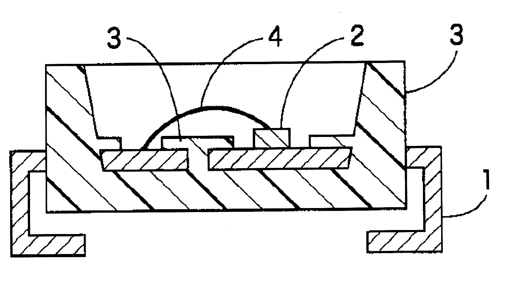
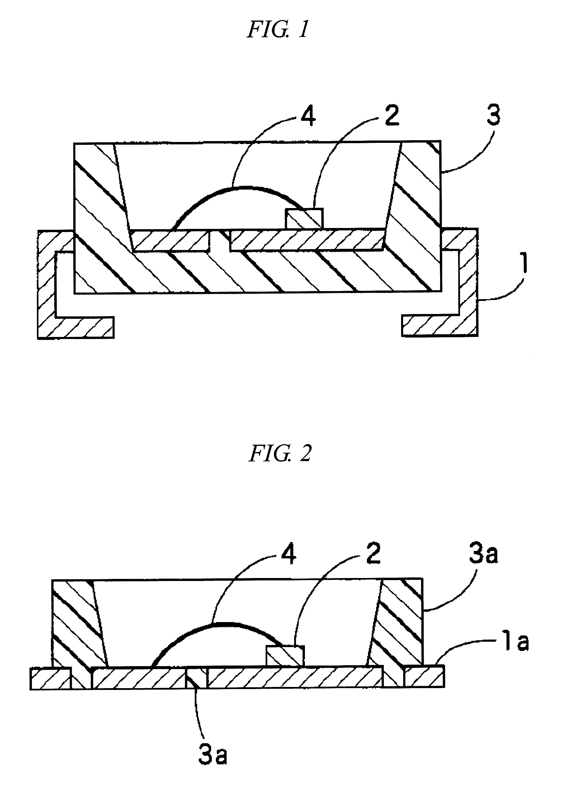
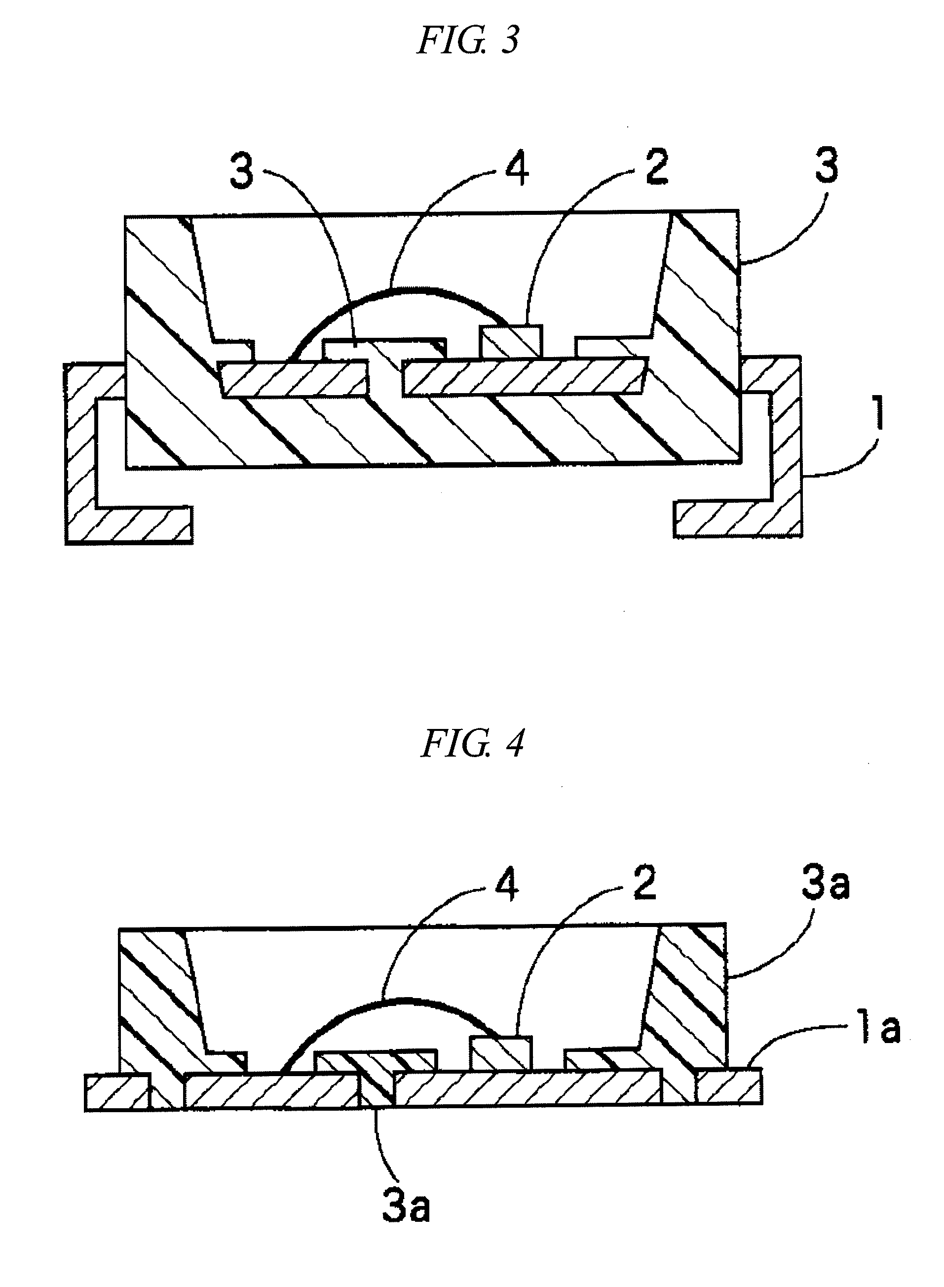
Image

Examples
examples
[0072]Next, Examples are given below together with Comparative Examples. However, it should not be construed that the invention is limited to these Examples.
[0073]First of all, prior to the fabrication of epoxy resin compositions, materials shown below were prepared.
[Epoxy Resin]
[0074]Triglycidyl isocyanurate (epoxy equivalent: 100)
[0075]Methylhexahydrophthalic anhydride (acid anhydride equivalent: 168)
[0076]Rutile type titanium oxide, average particle diameter: 0.2 μm
[Silica Powder]
[0077]Spherical fused silica, average particle diameter: 23 μm
[Release agent e1] (Example)
[0078]Compound having the structural formula (1) wherein k is 48; x is 20; and each of Rm and Rn is a hydrogen atom (UNITHOX 750, manufactured by Baker Petrolite Corporation)
example)
[Release agent e2] (Example)
[0079]Compound having the structural formula (1) wherein k is 28; x is 5; and each of Rm and Rn is a hydrogen atom (UNITHOX 420, manufactured by Baker Petrolite Corporation)
PUM
| Property | Measurement | Unit |
|---|---|---|
| Percent by mass | aaaaa | aaaaa |
| Percent by mass | aaaaa | aaaaa |
| Wavelength | aaaaa | aaaaa |
Abstract
Description
Claims
Application Information