Method of Stressing Static Random Access Memories for Pass Transistor Defects

a static random access memory and defect technology, applied in static storage, information storage, digital storage, etc., can solve the problems of increasing the likelihood of read and write functional failure, physical scaling of device size raises significant issues, and increases the variability of electrical characteristics, so as to efficiently distinguish vulnerable cells, without yield loss

Active Publication Date: 2013-02-14
TEXAS INSTR INC
View PDF4 Cites 24 Cited by
  • Summary
  • Abstract
  • Description
  • Claims
  • Application Information

AI Technical Summary

Benefits of technology

[0019]Embodiments of this invention provide such a method that efficiently distinguishes the vulnerable cells from good memory cells, without the yield loss due to over-screenin

Problems solved by technology

However, this physical scaling of device sizes raises significant issues, especially in connection with embedded SRAM but also in SRAM realized as “stand-alone” memory integrated circuit devices.
Several of these issues are due to increased variability in the electrical characteristics of transistors formed at these extremely small feature sizes.
This variability in characteristics has been observed to increase the likelihood of read and write functional failures, on a cell-to-cell basis.
The combination of increased device variability with the larger number of memory cells (and thus transistors) within an integrated circuit renders a high likelihood that one or more cells cannot be read or written as expected.
In general, a cell stability failure occurs if noise of sufficient magnitude couples to the bit lines of unselected cells, for example during a write to a selected memory cell in the same row, to cause a false write of data to unselected cells in that same row.
The possibility of such a cell stability failure is exacerbated by device mismatch and variability, as discussed above.
Write failures are the converse of cell stability failures—while a cell stability failure occurs if a cell changes its state too easily, a write failure occurs if an addressed cell is stubborn to being written with the opposite data state.
In general, write failures are due to the inability of write circuitry to pull dow

Method used


Image

  • Method of Stressing Static Random Access Memories for Pass Transistor Defects
  • Method of Stressing Static Random Access Memories for Pass Transistor Defects
  • Method of Stressing Static Random Access Memories for Pass Transistor Defects

Examples


Embodiment Construction

[0034]This invention will be described in connection with certain embodiments, namely as implemented into a method of testing static random access memories, because it is contemplated that this invention will be especially beneficial when used in such an application. However, it is also contemplated that this invention will also be beneficial if applied to memories of other types, and to stand-alone and embedded memories in integrated circuits of various architectures. Accordingly, it is to be understood that the following description is provided by way of example only, and is not intended to limit the true scope of this invention as claimed.

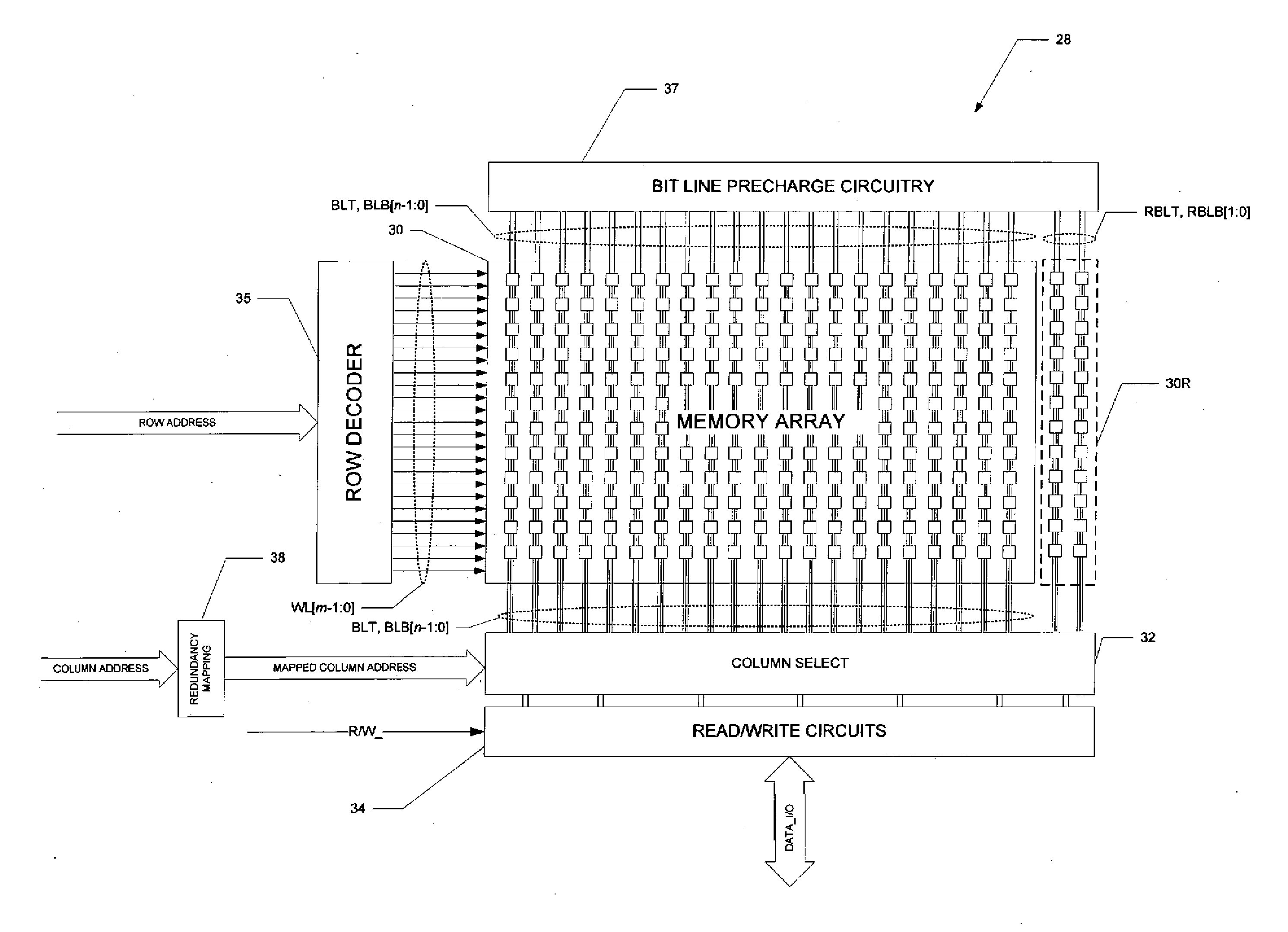
[0035]FIG. 2 illustrates an example of large-scale integrated circuit 20, in the form of a so-called “system-on-a-chip” (“SoC”), as now popular in many electronic systems. Integrated circuit 20 is a single-chip integrated circuit into which an entire computer architecture is realized. As such, in this example, integrated circuit 20 includes a ce...


PUM


Abstract

A method of stressing and screening static random access memory (SRAM) arrays to identify memory cells with bit line side pass transistor defects. After writing initial data states into the memory array under nominal bias conditions, an elevated bias voltage is applied to the memory array, for example to its power supply node. Under the elevated bias voltage, alternating data patterns are written into and read from the memory array for a selected duration. The elevated bias voltage is reduced, and a write screen is performed to identify defective memory cells. The dynamic stress of the repeated writes and reads accelerates early life failures, facilitating the write screen.

Description

CROSS-REFERENCE TO RELATED APPLICATIONS[0001]This application claims priority, under 35 U.S.C. §119(e), of Provisional Application No. 61 / 522,004, filed Aug. 10, 2011, which is incorporated herein by reference.STATEMENT REGARDING FEDERALLY SPONSORED RESEARCH OR DEVELOPMENT[0002]Not applicable.BACKGROUND OF THE INVENTION[0003]This invention is in the field of solid-state memory. Embodiments of this invention are more specifically directed to the manufacture and testing of static random access memories (SRAMs).[0004]Many modern electronic devices and systems now include substantial computational capability for controlling and managing a wide range of functions and useful applications. The computational power of these modern devices and systems is typically provided by one or more processor “cores”. These processor cores operate as a digital computer, in general retrieving executable instructions from memory, performing arithmetic and logical operations on digital data retrieved from m...

Claims


Application Information

Patent Timeline
IPC IPC(8): G11C29/00
CPCG11C11/41G11C29/06G11C29/50G11C29/00G11C29/08G11C11/419
Inventor RAVAL, JAYESH C.PIOUS, BEENAASHBURN, STANTON PETREEONDRUSEK, JAMES CRAIG
Owner TEXAS INSTR INC
Why Eureka
Try Eureka