Semiconductor Laser Device and a Method for Manufacturing a Semiconductor Laser Device

Inactive Publication Date: 2013-02-28
II VI LASER ENTERPRISE
View PDF6 Cites 13 Cited by
  • Summary
  • Abstract
  • Description
  • Claims
  • Application Information

AI Technical Summary

Benefits of technology

[0014]The use of ALD for the inner layer results in a layer having no pinholes and which therefore provides good moisture resistance. The outer layer

Problems solved by technology

This process leaves an entry path for moisture that causes failure in operation.
Even though standard passivation layers like SiN or Si3N4 deposited by plasma enhanced chemical vapour deposition (PECVD) may provide a moisture resistance sufficient to pass biased standard 85/85 tests, the devices show high failure rates in the harsher moisture sensitivity level (MSL-1) test, which includes unbiased pre-conditioning in wet environment.
The problem is believed to stem from pinholes which form in the passivation layer deposited after oxidation of the oxide layer, through which the moisture can penetrate.
Howeve

Method used


Image

  • Semiconductor Laser Device and a Method for Manufacturing a Semiconductor Laser Device
  • Semiconductor Laser Device and a Method for Manufacturing a Semiconductor Laser Device
  • Semiconductor Laser Device and a Method for Manufacturing a Semiconductor Laser Device

Examples


Embodiment Construction

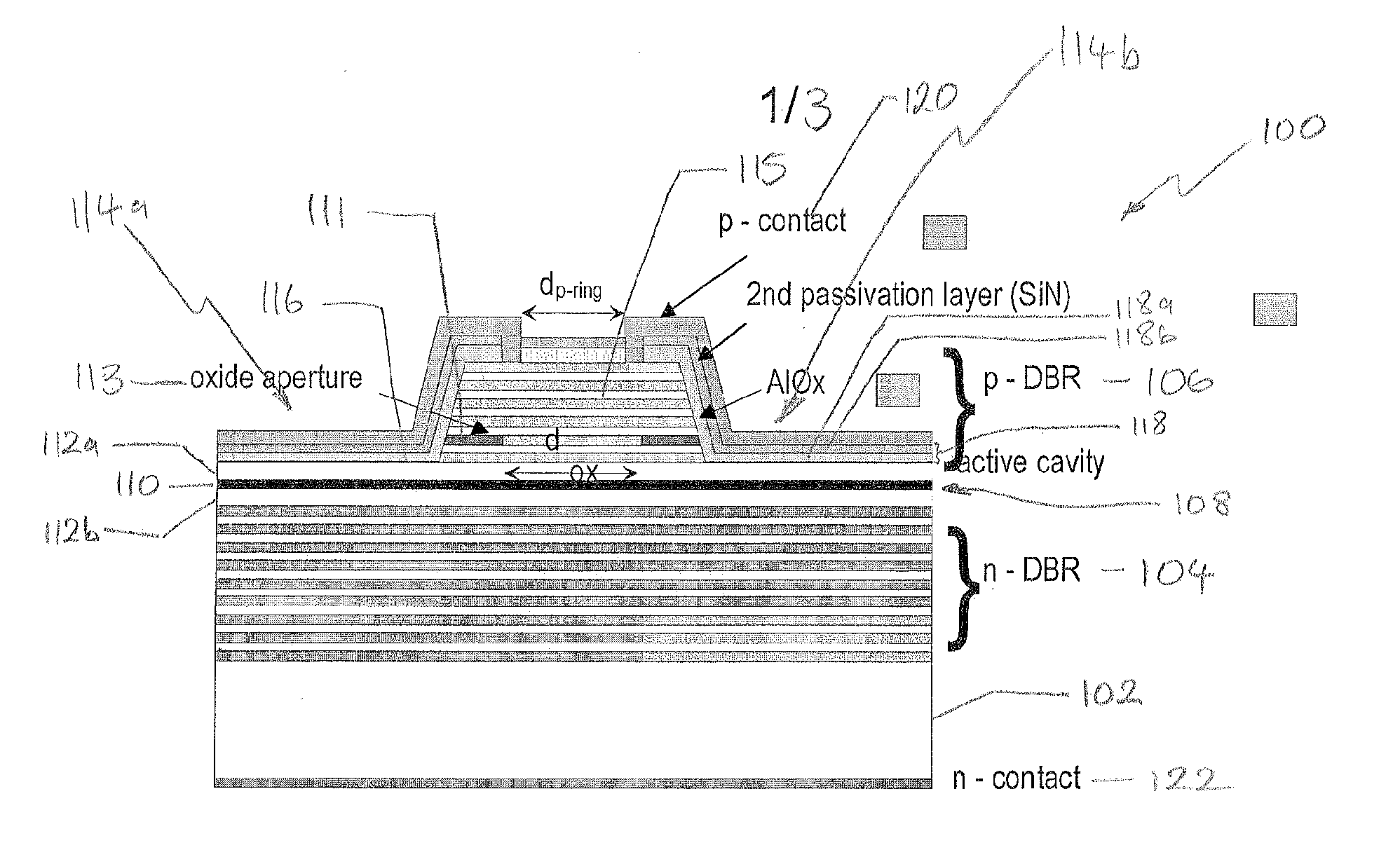
[0039]It has been shown that bulk diffusion is unlikely to be the penetration path for water ingress into a VCSEL device during 85 / 85 tests. It is more likely that pinholes in a passivation layer are the predominant penetration path. One solution for preventing pinhole diffusion is ALD deposition as ALD deposition results in no pinholes in the deposited material. However, ALD is an expensive process and takes a long time. Further, typical materials deposited by ALD, e.g. aluminum oxides, have an exothermic reaction with water.

[0040]Other common methods of providing a passivation layer for preventing moisture ingress to VCSEL devices, chemical vapour deposition (CVD) methods in particular, generate particles in the gas phase that deposit during film growth and lead to pinholes. The provision of two passivation layers deposited by CVD is not completely successful because both passivation layers still contain pinholes.

[0041]Stacks of PECVD Si3N4 thin films with various in-situ and ex-s...


PUM


Abstract

A semiconductor laser device formed on a semiconductor substrate, the device comprising: a passivation layer arranged on an upper surface of the device structure for resisting moisture ingress, wherein the passivation layer comprises an inner layer deposited on the upper surface of the device by atomic layer deposition and an outer layer deposited on the inner layer, and comprising a material that is inert in the presence of water.

Description

CROSS-REFERENCE TO RELATED APPLICATIONS[0001]This application claims benefit of U.S. provisional patent application Ser. No. 61 / 526,642, filed Aug. 23, 2011, and United Kingdom patent application number 1204836.9, filed Mar. 20, 2012, which are herein incorporated by reference.BACKGROUND OF THE INVENTION[0002]1. Field of the Invention[0003]The invention relates to a semiconductor laser device and a method for manufacturing a semiconductor laser device. In particular, the semiconductor laser device may be a vertical cavity surface-emitting laser device (VCSEL) or an edge emitting laser device having a passivation layer for resisting moisture ingress.[0004]2. Description of the Related Art[0005]In this specification, the term “light” will be used in the sense that it is used in optical systems to mean not just visible light, but also electromagnetic radiation having a wavelength outside that of the visible range.[0006]The vertical cavity surface emitting laser (VCSEL) has become an im...

Claims


Application Information

Patent Timeline
IPC IPC(8): H01S5/028H01L21/30
CPCH01S5/0282H01S5/0283H01S2301/176H01S5/18352H01S5/18369H01S5/18313
Inventor TRAUT, SILKESAINTENOY, STEPHANIE
Owner II VI LASER ENTERPRISE
Why Eureka
Try Eureka