Light source device and lighting device

Inactive Publication Date: 2013-03-07
STANLEY ELECTRIC CO LTD
View PDF8 Cites 50 Cited by
  • Summary
  • Abstract
  • Description
  • Claims
  • Application Information

AI Technical Summary

Benefits of technology

[0019]According to any of the above configurations, the light source device can be configured to include: the fixed light source that emits light of a predetermined wavelength within a wavelength region covering the wavelength of ultraviolet light and that of visible light; and the wavelength conversion layer or a fluorescent layer containing a wavelength conversion material of at least one type that is excited by excitation light from the fixed light source to emit fluorescent light of a wavelength longer than that of light emitted from the fixed light source. The fixed light source and the wavelength conversion layer can spatially be spaced from each other. The light source device can employ a reflection system of extracting at least fluorescent light from the surface of the wavelength conversion layer through which excitation light from the fixed light source can enter the wavelength conversion layer. Thus, the light source device can achieve brightness sufficiently higher than conventionally achieved brightness.
[0020]In particular, the wavelen

Problems solved by technology

However, the actual situation is such that heat is generated in the wavelength conversion layer to cause discoloration of a resin component or temperature quenching of a wavelength conversion material in the wavelength conversion layer, leading to reduction of the intensity of fluorescent light.
This may lead to saturation or reduction of the intensity of emitted light, making it difficult to increase the brightness of a light source device utilizing an optical semiconductor element and a wavelength conversion layer in combination.
Accordingly, if discolored with heat, the resin component absorbs part of the excitation light from an optical semiconductor element or fluorescent light fro

Method used


Image

  • Light source device and lighting device
  • Light source device and lighting device
  • Light source device and lighting device

Examples


Embodiment Construction

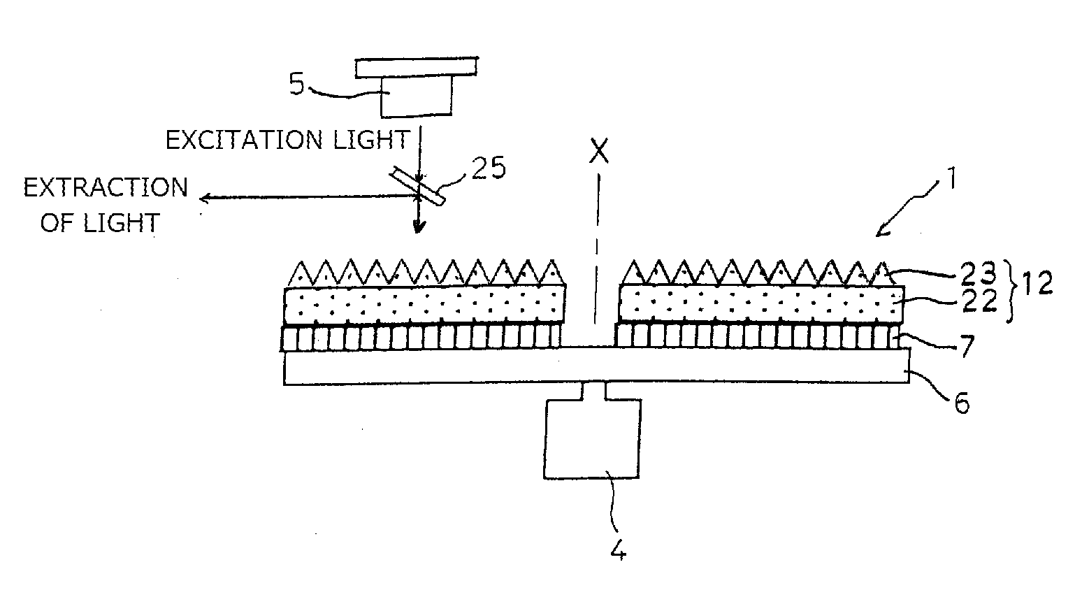
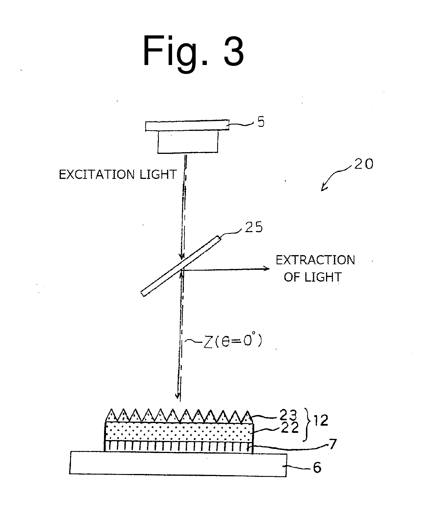
[0033]A description will now be made below to light source devices and lighting devices of the presently disclosed subject matter with reference to the accompanying drawings in accordance with exemplary embodiments.

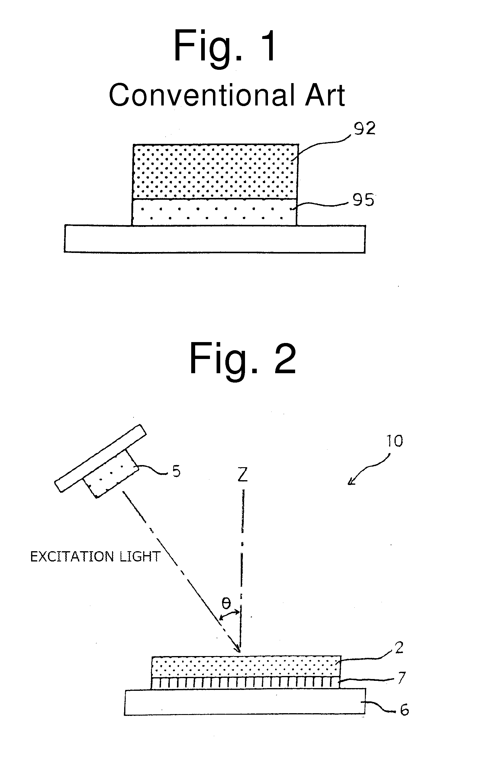
[0034]FIG. 2 shows a light source device described in an application (Japanese Patent Application No. 2009-286397) filed by the applicant of the instant application. Referring to FIG. 2, a light source device 10 can include a fixed light source 5 that emits light of a predetermined wavelength within a wavelength region covering the wavelength of ultraviolet light and that of visible light, and a fluorescent layer 2 (wavelength conversion layer) containing a fluorescent material (wavelength conversion material) of at least one type that is excited by excitation light from the fixed light source 5 to emit fluorescent light of a wavelength longer than that of light emitted from the fixed light source 5. The fixed light source 5 and the fluorescent layer 2 can spatially be sp...


PUM


Abstract

A light source can include: a light source that emits light of a predetermined wavelength within a wavelength region covering the wavelength of ultraviolet light and that of visible light; and a wavelength conversion layer containing a fluorescent material of at least one type that is excited by excitation light from the fixed light source to emit fluorescent light of a wavelength longer than that of light emitted from the fixed light source. The fixed light source and the wavelength conversion layer can be spaced from each other. The light source device can employ a reflection system of extracting at least fluorescent light from an incident surface of the wavelength conversion layer through which excitation light from the fixed light source enters the wavelength conversion layer. The wavelength conversion layer can have a surface structure with depressions or projections.

Description

[0001]This application claims the priority benefit under 35 U.S.C. §119 of Japanese Patent Application No. 2011-113546 filed on May 20, 2011, which is hereby incorporated in its entirety by reference.TECHNICAL FIELD[0002]The presently disclosed subject matter relates to a light source device and a lighting device.BACKGROUND ART[0003]A light source device using an optical semiconductor element such as an LED and a wavelength conversion layer such as a fluorescent layer in combination has been in widespread use. As a result of recent trends toward higher brightness, such a light source device has been applied in a wider range of applications including general lighting and in automobile and other vehicle headlights. This type of light source device is considered to be able to provide a wider range of applications if it continues to increase in terms of its brightness.[0004]The brightness of the aforementioned light source device using an optical semiconductor element and a wavelength c...

Claims


Application Information

Patent Timeline
IPC IPC(8): H01L33/50
CPCF21V9/16G02F1/00F21S48/1317F21S48/1145F21Y2101/02F21V13/08F21Y2115/10F21S41/16F21S41/176F21S41/32F21V9/30F21V9/45
Inventor KAWAKAMI, YASUYUKI
Owner STANLEY ELECTRIC CO LTD
Why Eureka
Try Eureka