Providing group v and group vi over pressure for thermal treatment of compound semiconductor thin films

a technology of compound semiconductor and overpressure, which is applied in the direction of semiconductor devices, electrical appliances, basic electric elements, etc., can solve the problems of increasing growing a low resistivity, and unsatisfactory desired doping profiles, so as to prevent the loss of group v crystallinity, and reduce the cost of ownership

Inactive Publication Date: 2013-03-07
APPLIED MATERIALS INC
View PDF6 Cites 30 Cited by
  • Summary
  • Abstract
  • Description
  • Claims
  • Application Information

AI Technical Summary

Benefits of technology

[0009]The present invention generally provide methods for forming high quality, low resistivity Group III-V or Group II-VI compounds with high concentration of Group V or VI material formed at or near the surface of Group III-V or Group II-VI compounds to help prevent loss of crystallinity of Group V or VI elements at or near the surface. In one embodiment, a method of manufacturing a compound semiconductor includes growing a compound semiconductor layer having a n-type or p-type dopant over a substrate, the compound semiconductor layer comprising at least a first component and a second component, wherein the second component has a vapor pressure relatively higher than the first component, forming a supplemental layer consisted essentially of the second component at or near an upper surface of the compound semiconductor layer, and subjecting the substrate to an annealing process. The compound semiconductor layer may be n-type or p-type Group III-V or Group II-VI compound semiconductors. In one example, a capping layer may be optionally formed on the supplemental layer to help prevent loss of crystallinity of the second component at elevated temperatures. An overpressure of the second component gas may be provided onto an exposed surface of the substrate during annealing to enhance the surface morphology of the compound semiconductor layer.
[0011]In yet another embodiment, a method of manufacturing a compound semiconductor includes growing a Group III-V compound semiconductor layer over a substrate, forming a p-type doping layer on an upper surface of the Group III-V compound semiconductor layer, forming a supplemental layer consisted essentially of Group V material on the p-type doping layer, forming a capping layer on the supplemental layer, and subjecting the substrate to an annealing process. In one example, an overpressure of the second component gas onto an exposed surface of the substrate during annealing to enhance the surface morphology of the Group III-V compound semiconductor layer.

Problems solved by technology

However, growing a low resistivity, high quality p-type Group III-V compound on a substrate of a different material, such as a sapphire substrate or a silicon substrate, with a desired doping profile has been unsatisfactory.
While surface decomposition can be suppressed or at least reduced by providing an overpressure of nitrogen in a thermal annealing chamber, utilization of overpressure undesirably increases the cost of ownership since it would require high ambient concentration in the gas surrounding the substrate along with safety related containment and monitoring.
In addition, efforts to dope the GaN film p-type have been unsuccessful since GaN is naturally an n-type doped semiconductor material with high carrier concentration.
Many devices require a free carrier concentration in the p-type doped GaN of at least 1018 cm−3; however, Mg-doped GaN is suffering from insufficient carrier concentration since the effect of a dopant impurity (e.g., Mg) is greatly reduced by high amount of nitrogen vacancies as discussed above and in most situations is “neutralized” or “inactivated” by unintentional H passivation due to the formation of Mg—H complexes (if NH3 gas is used during the process to contribute the N component).
Therefore, only a few percent of Mg dopant atoms are activated, which contributes to non-ideal tradeoffs in structure, composition, and device performance.

Method used


Image

  • Providing group v and group vi over pressure for thermal treatment of compound semiconductor thin films
  • Providing group v and group vi over pressure for thermal treatment of compound semiconductor thin films
  • Providing group v and group vi over pressure for thermal treatment of compound semiconductor thin films

Examples


Embodiment Construction

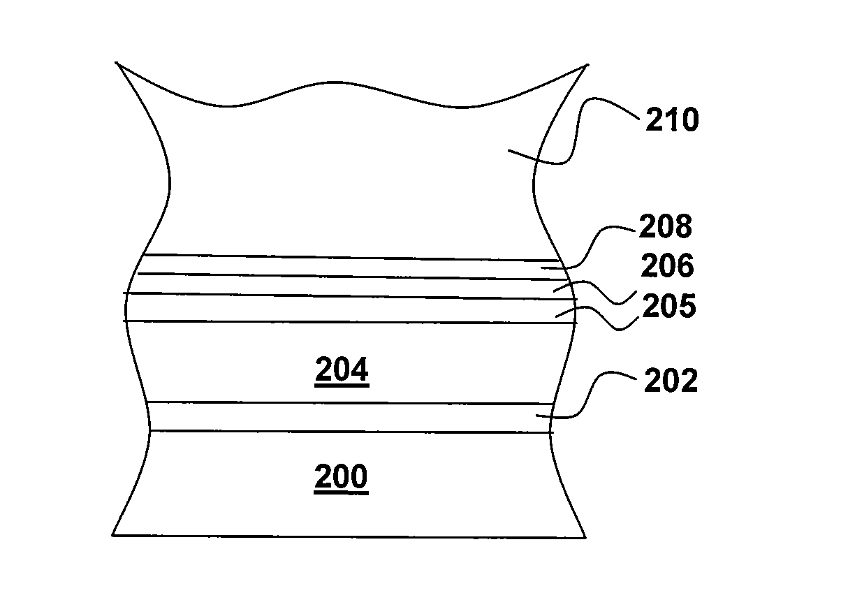
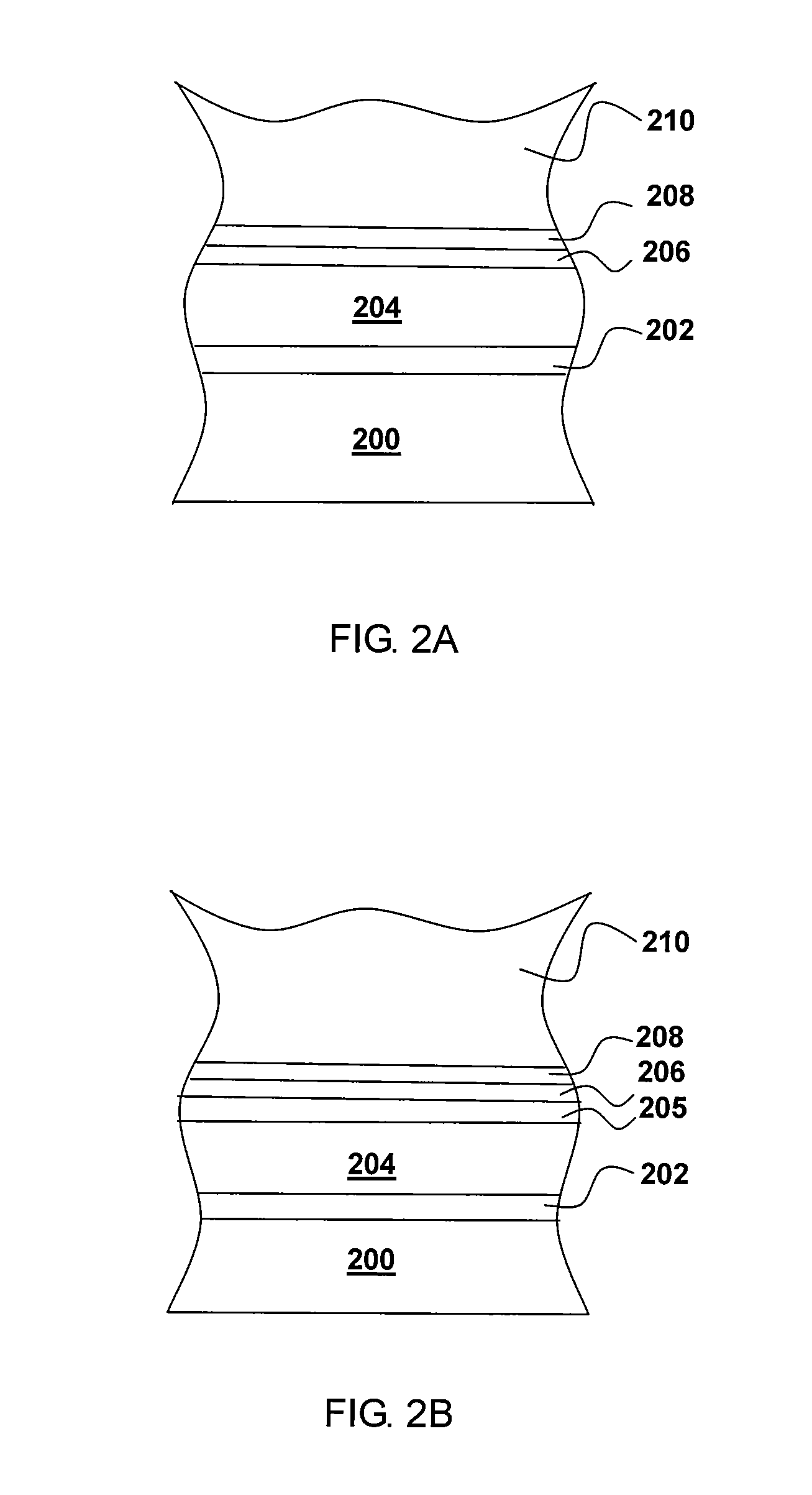
[0019]Embodiments disclosed herein generally provide methods for forming high quality, low resistivity Group III-V or Group II-VI compounds with high concentration of Group V or VI material formed at or near the surface of Group III-V or Group II-VI compounds to help prevent loss of crystallinity of Group V or VI elements at or near the surface at elevated temperatures. The surface morphology and the lattice quality may be improved by use of a capping layer deposited on top of the high concentration of Group V or VI material and additionally an overpressure of Group V or VI material gas provided onto the exposed surface of the substrate during a subsequent annealing process to prevent surface decomposition or other stoichiometric degradation of the crystal near the surface of the Group III-V or II-VI compound layer.

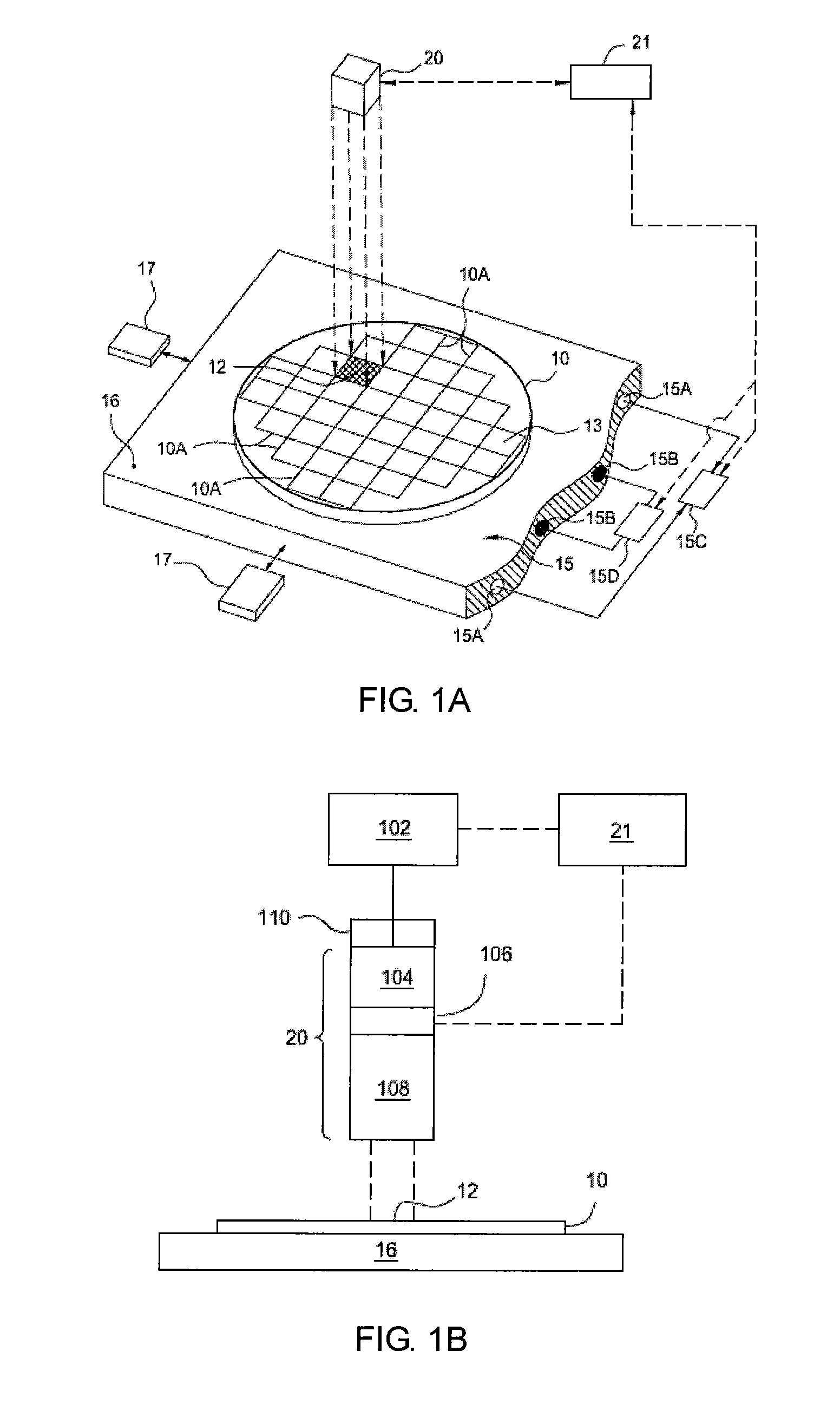
[0020]FIG. 1A illustrates an isometric view of one embodiment of the invention that may be used to benefit the present invention. In one embodiment, an energy source 20 i...


PUM

PropertyMeasurementUnit
energyaaaaaaaaaa
wavelengthaaaaaaaaaa

Abstract

Embodiments of the invention provide methods for forming high quality, low resistivity Group III-V or Group II-VI compounds. In one embodiment, the method includes growing a compound semiconductor layer having a n-type or p-type dopant over a substrate, the compound semiconductor layer comprising at least a first component and a second component, and the second component has a vapor pressure relatively higher than the first component, forming a supplemental layer consisted essentially of the second component at or near an upper surface of the compound semiconductor layer, and anneal the substrate. A capping layer may be formed on the supplemental layer to help prevent loss of crystallinity of the second component at elevated temperatures. An overpressure of the second component gas may be provided onto an exposed surface of the substrate during annealing to enhance the surface morphology of the compound semiconductor layer.

Description

CROSS-REFERENCE TO RELATED APPLICATIONS[0001]This application claims benefit of U.S. provisional patent application Ser. No. 61 / 531,885, filed Sep. 7, 2011, which is herein incorporated by reference.BACKGROUND OF THE INVENTION[0002]1. Field of the Invention[0003]Embodiments of the present invention generally relate to processes for forming low resistivity Group III-V or Group II-VI compound semiconductors with high doping concentration at or near the surface of Group III-V or Group II-VI compound semiconductors.[0004]2. Description of the Related Art[0005]Group III-V or II-V compounds are finding greater importance in the development and fabrication of a variety of semiconductor devices, such as light emitting diodes (LEDs), laser diodes (LDs), and logic circuit devices such as field effect transistors (FETs). In these devices, a plurality of semiconductor layers having different mixed crystal compositions are layered together to obtain intended optical and electrical characteristic...

Claims


Application Information

Patent Timeline
Patent Type & Authority Applications(United States)
IPC IPC(8): H01L21/20H01L29/267
CPCH01L21/0237H01L21/02538H01L21/0254H01L21/26546H01L21/02573H01L21/0262H01L21/02551
Inventor SRINIVASAN, SWAMINATHAN T.
Owner APPLIED MATERIALS INC
Why Eureka
Try Eureka