Impedance matching ground plane for high efficiency coupling with optical antennas

Inactive Publication Date: 2013-03-07
RGT UNIV OF CALIFORNIA
View PDF1 Cites 10 Cited by
  • Summary
  • Abstract
  • Description
  • Claims
  • Application Information

AI Technical Summary

Benefits of technology

[0013]An apparatus and method are described for a metallic ground plane for increasing coupling efficiency for optical nanoantennas. The ground plane can be utilized in vari

Problems solved by technology

However, it is difficult to achieve e

Method used


Image

  • Impedance matching ground plane for high efficiency coupling with optical antennas
  • Impedance matching ground plane for high efficiency coupling with optical antennas
  • Impedance matching ground plane for high efficiency coupling with optical antennas

Examples


embodiment 1

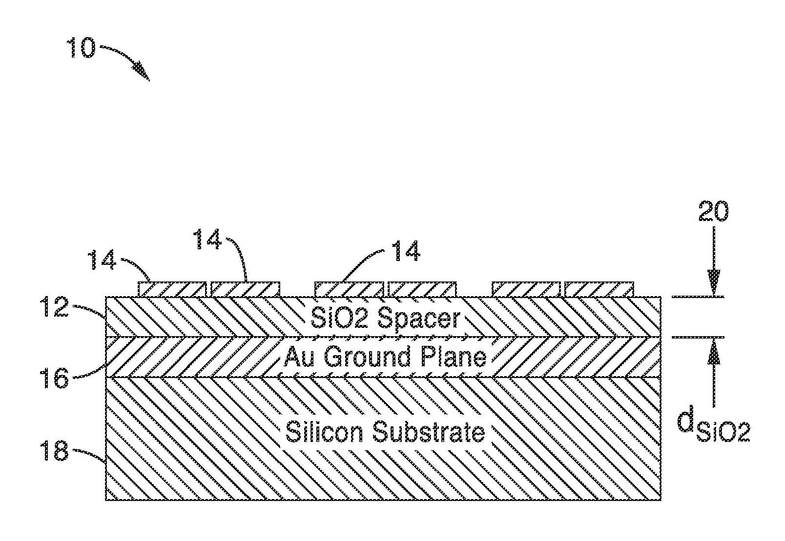
[0052]2. The apparatus of embodiment 1, wherein said dielectric spacer layer comprises SiO2.

[0053]3. The apparatus of embodiment 1, wherein said metallic layer comprises Au.

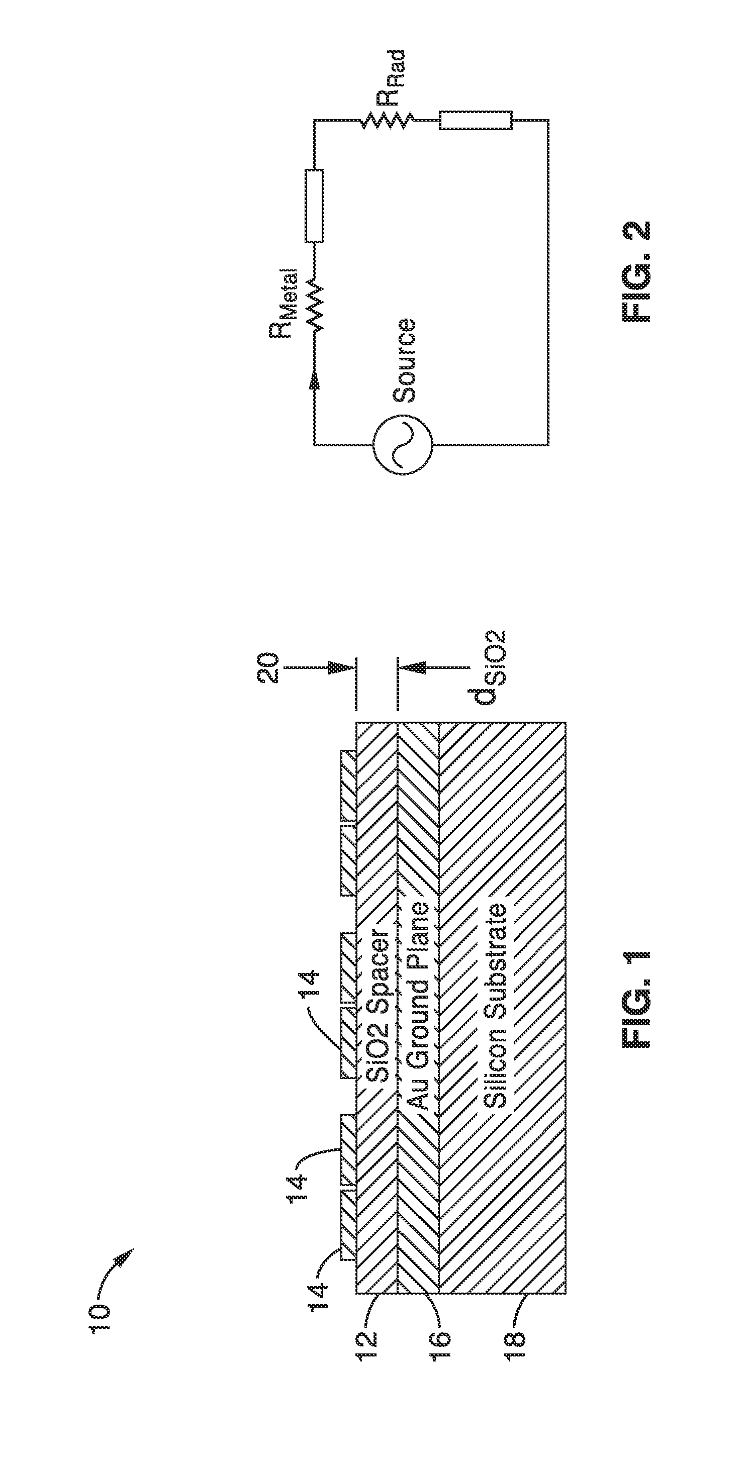
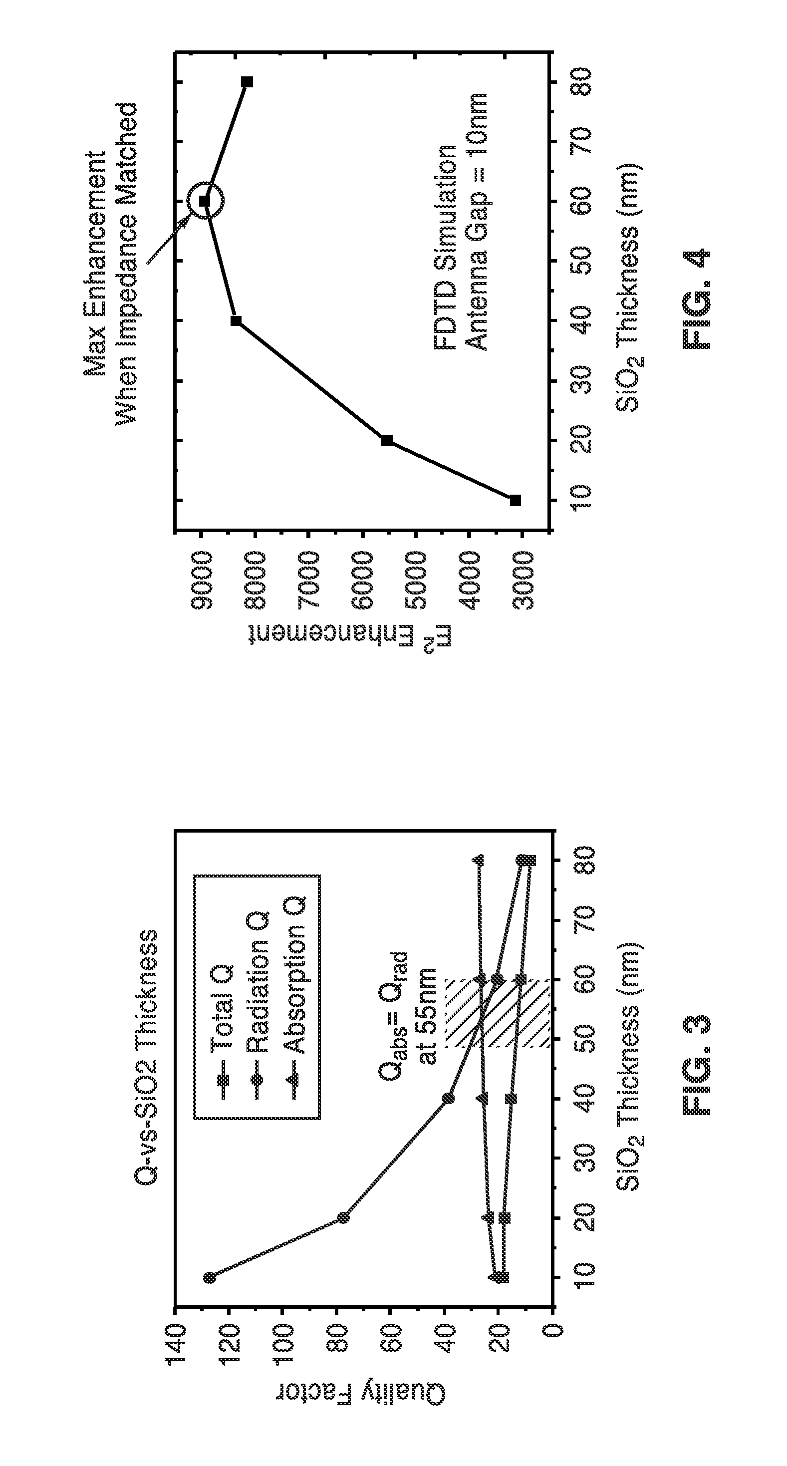
[0054]4. The apparatus of embodiment 1, wherein metal loss resistance and radiation resistance of the optical nanoantenna layer for a given optical antenna configuration and operating wavelength is matched when radiation quality factor and absorption quality factor are equal.

[0055]5. The apparatus of embodiment 1, wherein said dielectric spacer thickness is determined in response to finite difference time domain (FDTD) simulations.

[0056]6. The apparatus of embodiment 1, wherein said optical nanoantenna ground plane apparatus enhances field intensity by multiple times over using a glass substrate as a ground plane.

embodiment 6

[0057]7. The apparatus of embodiment 6, wherein said multiple times comprises five times.

[0058]8. The apparatus of embodiment 1, wherein said optical nanoantenna ground plane apparatus enhances surface-enhanced Raman spectroscopy (SERS) by more than an order of magnitude in comparison to optical antennas fabricated over a glass substrate.

embodiment 8

[0059]9. The apparatus of embodiment 8, wherein said more than an order of magnitude comprises an increase by a factor of approximately thirty.

[0060]10. The apparatus of embodiment 1, wherein said dielectric comprises trans-1,2-bis ethylene (BPE) deposited on optical nanoantennas of the optical antenna layer.

[0061]11. An optical antenna ground plane apparatus, comprising: a metallic layer disposed as a ground plane proximal to an optical nanoantenna layer; and a dielectric spacer layer of a selected thickness disposed between said metallic layer and the optical nanoantenna layer; wherein the thickness of said dielectric spacer layer is determined in response to matching metal loss resistance and radiation resistance of the optical nanoantenna layer for a given optical nanoantenna configuration and operating wavelength; wherein metal loss resistance and radiation resistance of the optical nanoantenna layer for a given optical nanoantenna configuration and operating wavelength is matc...


PUM

PropertyMeasurementUnit
Thicknessaaaaaaaaaa
Dielectric polarization enthalpyaaaaaaaaaa
Electrical resistanceaaaaaaaaaa

Abstract

An optical nanoantenna ground plane apparatus and method which enhances electric field intensity, surface-enhanced Raman spectroscopy (scattering). A dielectric spacer layer is disposed between a nanoantenna layer and a metallic ground plane layer. Thickness of the dielectric spacer layer is determined in response to matching metal loss resistance and radiation resistance of the optical nanoantenna layer for a given optical antenna configuration and operating wavelength, such as in response to finite difference time domain (FDTD) simulations which determine dielectric spacer layer thickness when radiation quality factor and absorption quality factor are equal. The inventive ground plane can be implemented for a wide range of optical applications regardless of whether fabrication of the nanoantenna-groundplane combination is fabricated in a top-down or bottom-up sequence.

Description

CROSS-REFERENCE TO RELATED APPLICATIONS[0001]This application a 35 U.S.C. §111(a) continuation of PCT international application number PCT / US2011 / 034219 filed on Apr. 27, 2011, incorporated herein by reference in its entirety, which is a nonprovisional of U.S. provisional patent application Ser. No. 61 / 329,059 filed on Apr. 28, 2010, incorporated herein by reference in its entirety.[0002]The above-referenced PCT international application was published as PCT International Publication No. WO 2012 / 011998 on Jan. 26, 2012 and republished on Apr. 26, 2012, and is incorporated herein by reference in its entirety.STATEMENT REGARDING FEDERALLY SPONSORED RESEARCH OR DEVELOPMENT[0003]This invention was made with Government support under Grant No. FA9550-08-1-0257 awarded by DARPA SERS S&T Fundamentals. The Government has certain rights in the invention.INCORPORATION-BY-REFERENCE OF MATERIAL SUBMITTED ON A COMPACT DISC[0004]Not ApplicableNOTICE OF MATERIAL SUBJECT TO COPYRIGHT PROTECTION[0005...

Claims


Application Information

Patent Timeline
IPC IPC(8): G01J3/44H01P11/00
CPCY10T29/49016G01N21/658
Inventor JAMSHIDI, ARASHSEOK, TAE JOONKIM, MYUNGKILAKHANI, AMITWU, MING C.
Owner RGT UNIV OF CALIFORNIA
Why Eureka
Try Eureka