Fluorine Implant Under Isolation Dielectric Structures to Improve Bipolar Transistor Performance and Matching

Active Publication Date: 2013-03-14
TEXAS INSTR INC
View PDF1 Cites 1 Cited by
  • Summary
  • Abstract
  • Description
  • Claims
  • Application Information

AI Technical Summary

Benefits of technology

This patent describes a method and transistors that increase the forward-active current gain compared to conventional bipolar transistors. This method is not affected by subsequent plasma etching processes and ensures a more matched performance among bipolar transistors in the same integrated circuit. It also minimizes any impact on the electrical characteristics of other transistors, such as MOS logic transistors, in the same circuit. The method involves applying a masked fluorine implant to the silicon surface at the locations of isolation structures, such as shallow trench isolation structures or local oxidation of silicon. The fluorine implant is believed to seal charge trapping sites that otherwise require a component of base current to charge and de-charge during transistor operation.

Problems solved by technology

However, the causal relationship between a manufacturing process and the resulting transistor performance parameter is not readily apparent in some cases.
In some cases, the causal relationship between a process change and a widespread degradation in transistor performance can be quite puzzling.
Degradation of transistor performance and increased variation in operating parameters are, of course, undesirable.
However, some circuits are especially vulnerable to mismatch in device parameters among transistors within the same integrated circuit.
It has been observed that the implementation of copper metallization not only degrades the circuit performance of bipolar transistors due to reduced transistor gain as mentioned above, but also increases transistor mismatch (in both the hFE and VBE values) among bipolar transistors in the same circuit.

Method used


Image

  • Fluorine Implant Under Isolation Dielectric Structures to Improve Bipolar Transistor Performance and Matching
  • Fluorine Implant Under Isolation Dielectric Structures to Improve Bipolar Transistor Performance and Matching
  • Fluorine Implant Under Isolation Dielectric Structures to Improve Bipolar Transistor Performance and Matching

Examples


Embodiment Construction

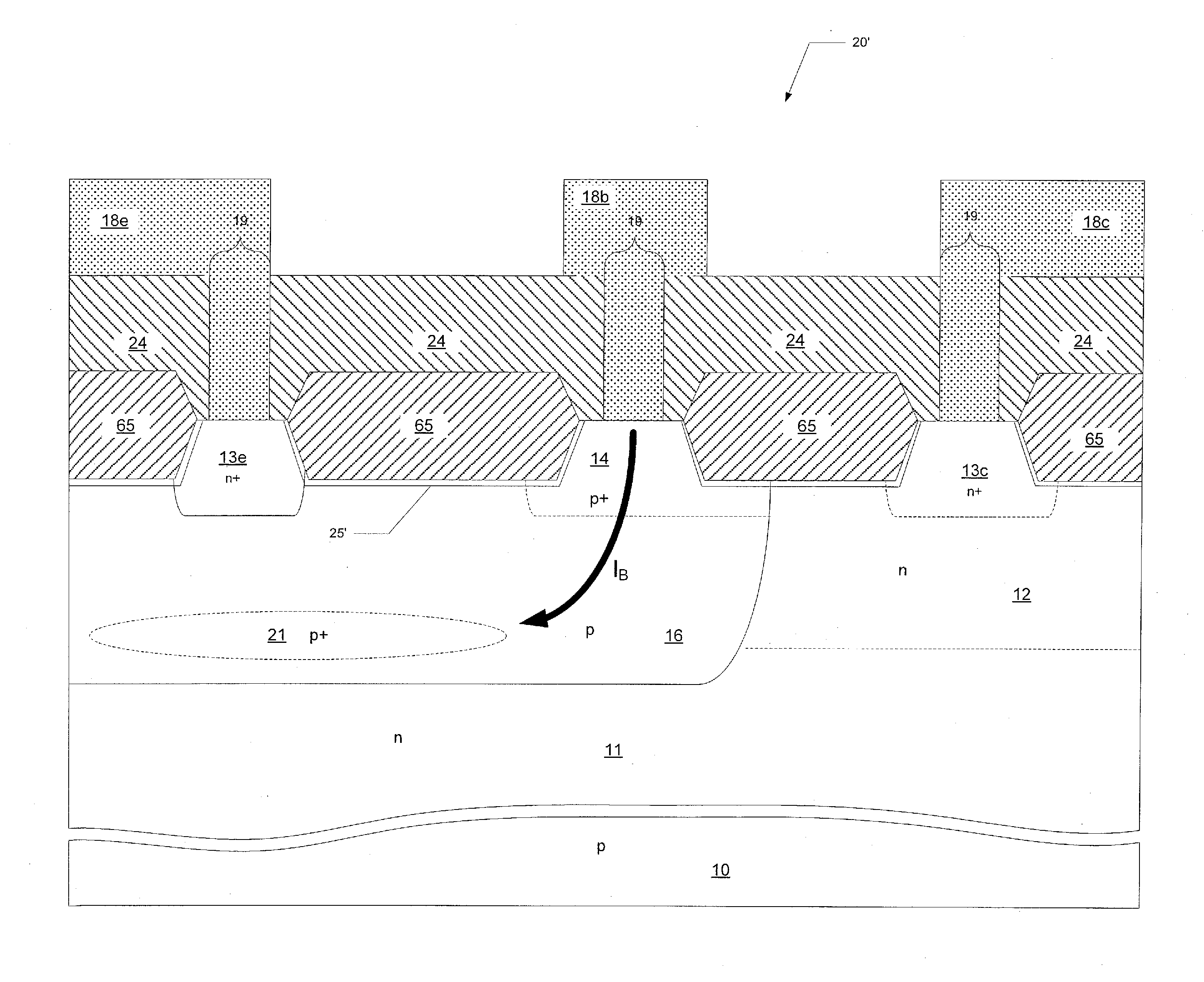
[0024]This invention will be described in connection with its embodiments, namely as implemented into a process of fabricating a silicon integrated circuit including bipolar transistors, as it is contemplated that this invention is especially beneficial in such an application. It is further contemplated, however, that this invention may be beneficially applied to the fabrication of a wide range of integrated circuits beyond those described herein. Accordingly, it is to be understood that the following description is provided by way of example only, and is not intended to limit the true scope of this invention as claimed.

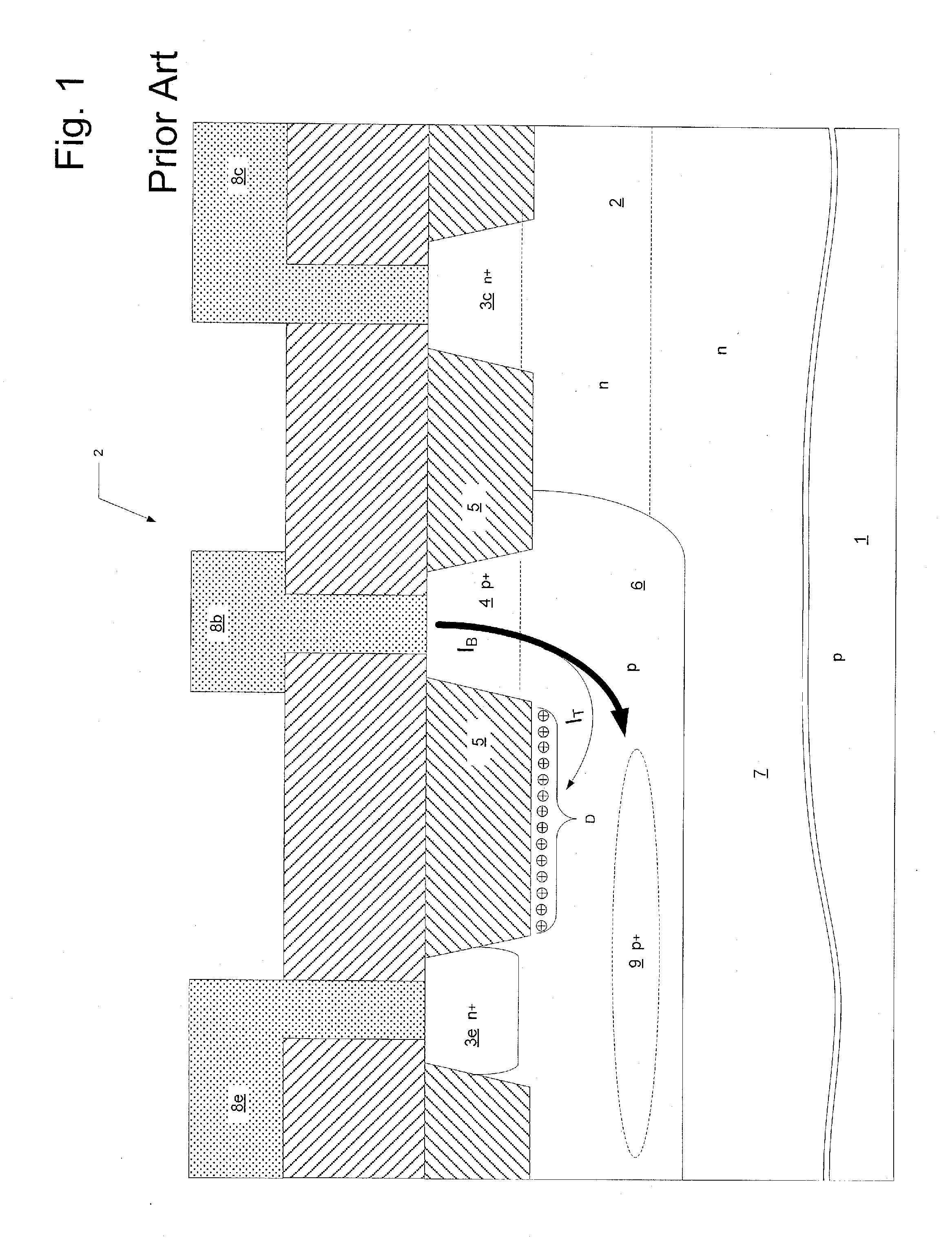
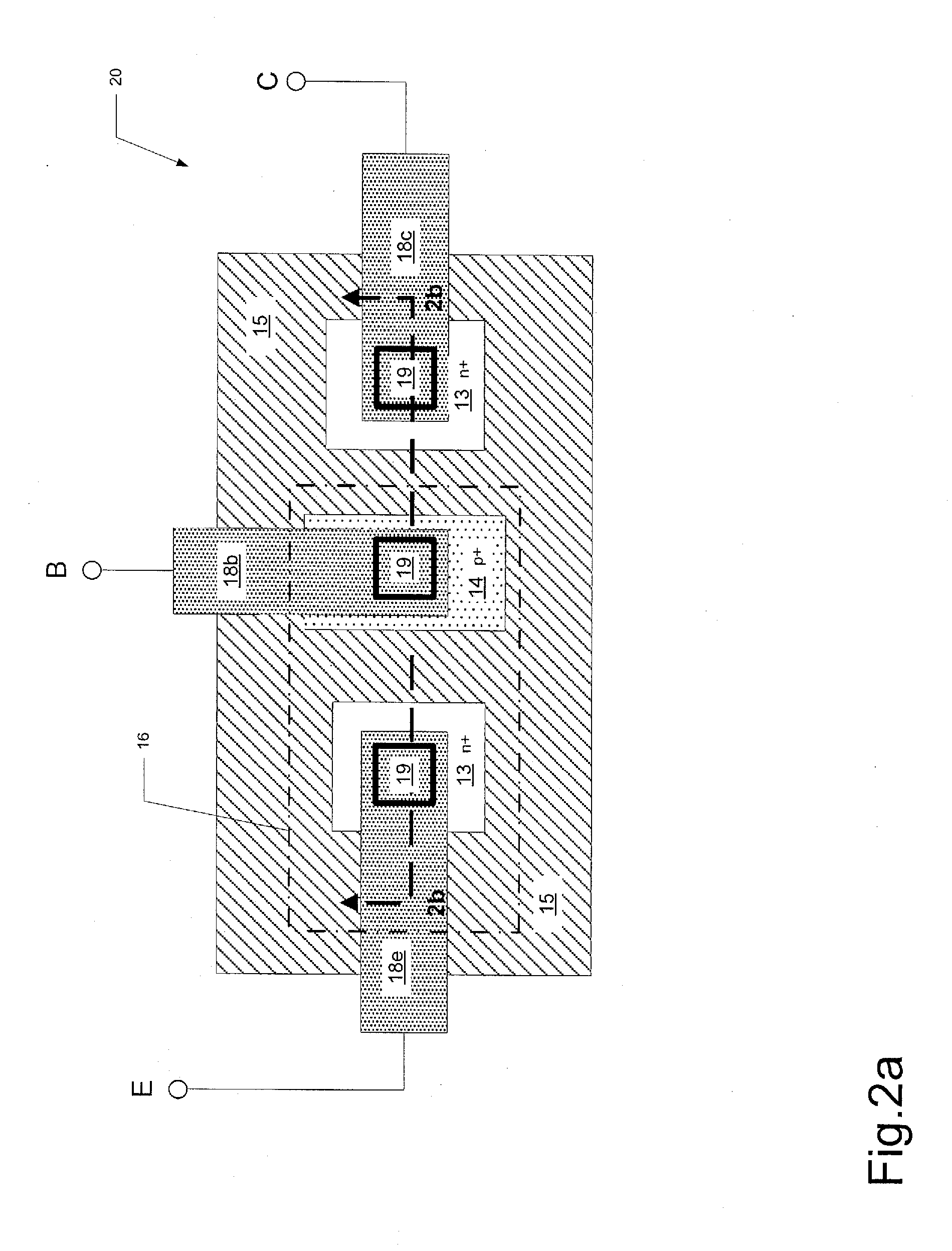
[0025]FIG. 1 illustrates, in cross-section, the structure of conventional n-p-n bipolar transistor 2. In this conventional construction, transistor 2 is formed at the surface of a silicon substrate, with metal conductors 8e, 8b, 8c serving as the transistor emitter, base, and collector electrodes. In this vertical n-p-n construction, conductor 8e makes contact to hea...


PUM


Abstract

A method of fabricating an integrated circuit including bipolar transistors that reduces the effects of transistor performance degradation and transistor mismatch caused by charging during plasma etch, and the integrated circuit so formed. A fluorine implant is performed at those locations at which isolation dielectric structures between base and emitter are to be formed, prior to formation of the isolation dielectric. The isolation dielectric structures may be formed by either shallow trench isolation, in which the fluorine implant is performed after trench etch, or LOCOS oxidation, in which the fluorine implant is performed prior to thermal oxidation. The fluorine implant may be normal to the device surface or at an angle from the normal. Completion of the integrated circuit is then carried out, including the use of relatively thick copper metallization requiring plasma etch.

Description

CROSS-REFERENCE TO RELATED APPLICATIONS[0001]This application claims priority, under 35 U.S.C. §119(e), of Provisional Application No. 61 / 532,845, filed Sep. 9, 2011, incorporated herein by this reference.STATEMENT REGARDING FEDERALLY SPONSORED RESEARCH OR DEVELOPMENT[0002]Not applicable.BACKGROUND OF THE INVENTION[0003]This invention is in the field of the manufacture of semiconductor integrated circuits. Embodiments of this invention are more specifically directed to the fabrication of isolation structures at the locations of bipolar transistors in semiconductor integrated circuits.[0004]As fundamental in the art, an important parameter related to the performance of bipolar junction transistors is the common-emitter current gain, or forward-active current gain. This parameter is commonly symbolized as β or βF, according to the Ebers-Moll model terminology; in the h-parameter model terminology, the bipolar transistor current gain is referred to as hFE. This current gain hFE is calc...

Claims


Application Information

Patent Timeline
IPC IPC(8): H01L21/331
CPCH01L29/66272H01L29/1004H01L29/732
Inventor TIAN, WEIDONGCHUANG, MING-YEHAGGARWAL, RAJNI J.
Owner TEXAS INSTR INC
Why Eureka
Try Eureka