Sputter deposition apparatus

a technology of sputter and sputter blade, which is applied in the direction of vacuum evaporation coating, electrolysis components, coatings, etc., can solve the problems of arcing and abnormal discharge, and achieve the effects of preventing damage to the target due to arcing, improving the efficiency of target use, and prolonging the life of the targ

Inactive Publication Date: 2013-03-21
ULVAC INC
View PDF5 Cites 1 Cited by
  • Summary
  • Abstract
  • Description
  • Claims
  • Application Information

AI Technical Summary

Benefits of technology

[0022]Since sputtering can be carried out across the entire sputtering surface of the target, the usage efficiency of the target can be improved and the life of the target can be extended.
[0023]Since insulant does not accumulate on the electrically-conductive target, arcing does not occur, damage to the target due to arcing can be prevented, and contamination due to impurities in the thin film to be formed can be prevented.
[0024]Since the space between the outer peripheries of adjacent targets can be widened, the amount of target material to be used can be reduced; and thus, the cost can be reduced.

Problems solved by technology

This has been a problem because electrical charge builds up on the insulating thin films, and it makes the insulating thin films to cause insulation breakdown at locations where the electrical charge amount exceeds a certain threshold; and thus, electrical current suddenly flows to the targets 1211 to 1214 and causes abnormal discharge (arcing) (see, for example, JPAH04-210471).

Method used


Image

  • Sputter deposition apparatus
  • Sputter deposition apparatus
  • Sputter deposition apparatus

Examples


Embodiment Construction

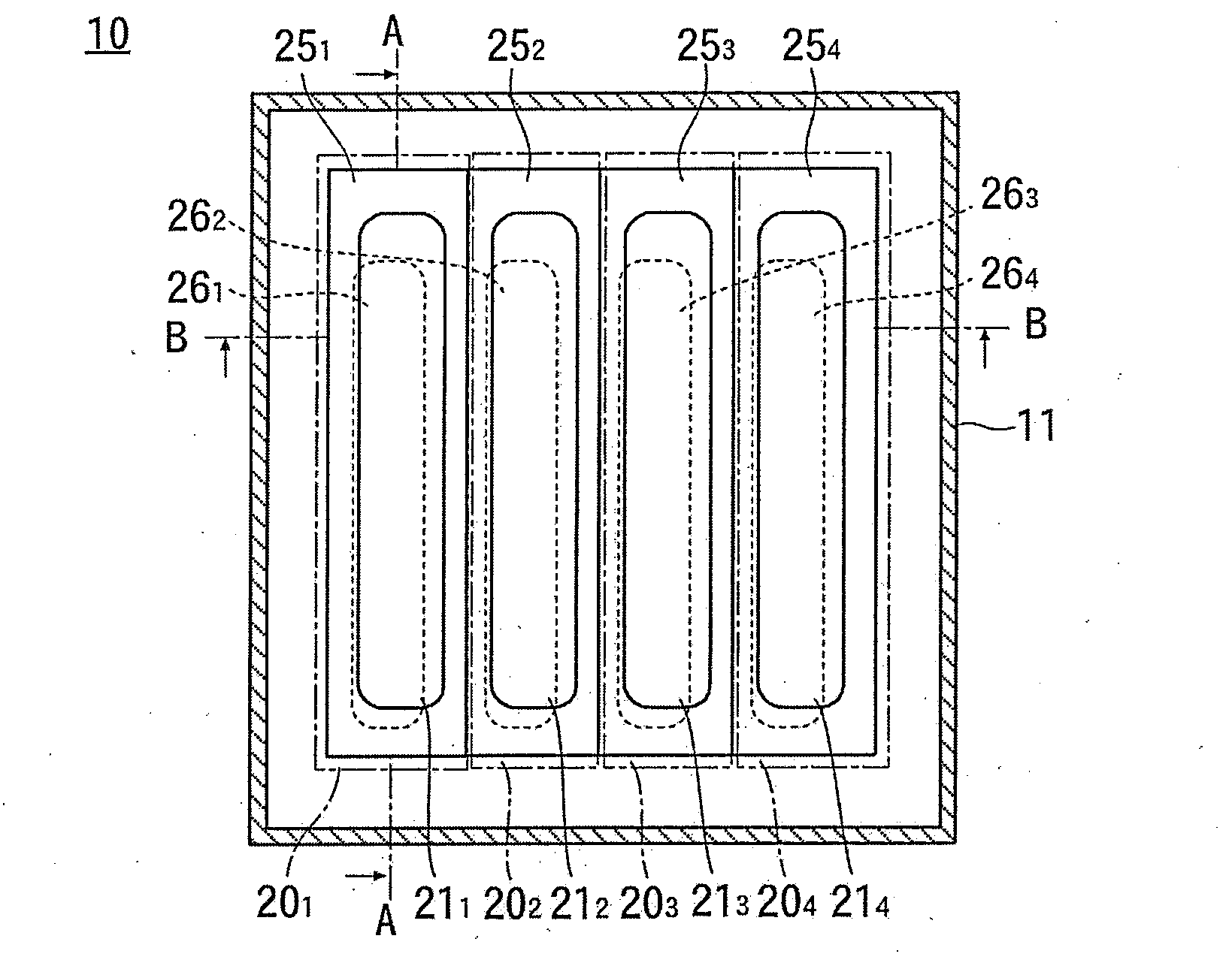
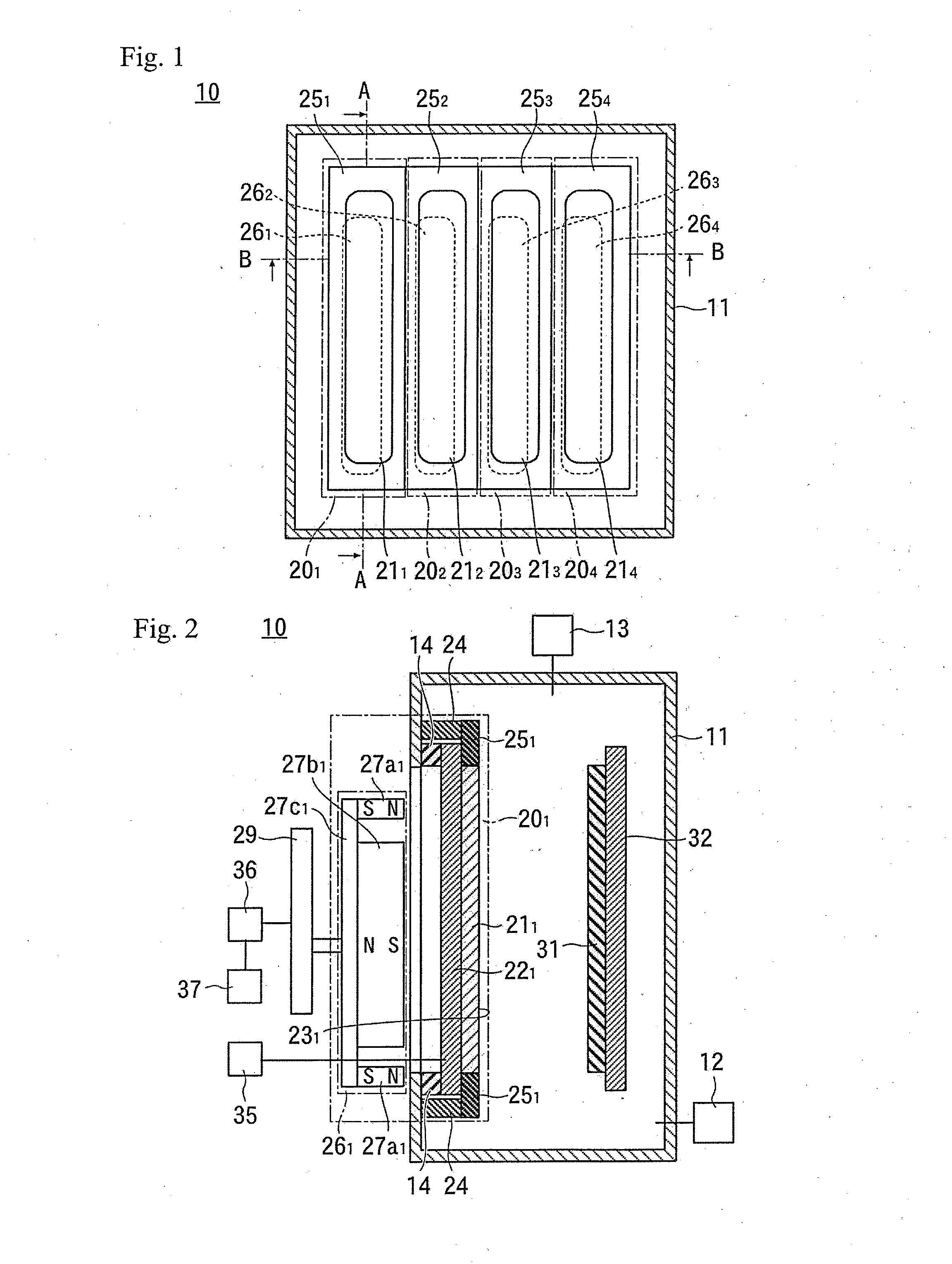
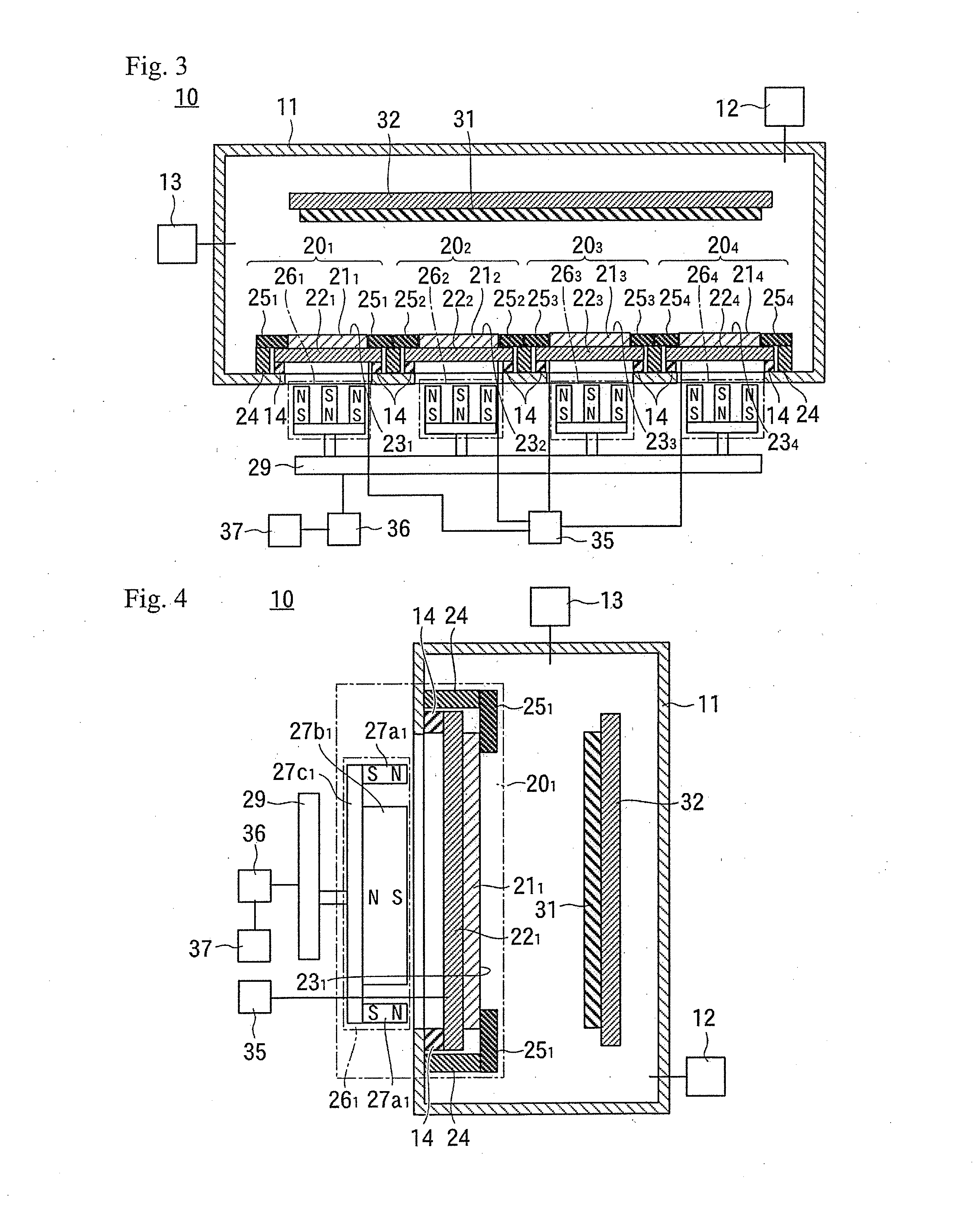
[0033]The structure of the sputter deposition apparatus of the present invention will now be explained.

[0034]FIG. 1 is an internal structure view of a sputter deposition apparatus 10; FIG. 2 is a cross-sectional view along line A-A of FIG. 1, and FIG. 3 is a cross-sectional view along line B-B of FIG. 1.

[0035]The sputter deposition apparatus 10 includes a vacuum chamber 11 and a plurality of sputter units 201 to 204.

[0036]The structure of the sputter units 201 to 204 is the same. The following explanation uses the sputter unit associated with reference numeral 201 as a representative example.

[0037]The sputter unit 201 includes a target 211 having a sputtering surface 231 which is exposed inside the vacuum chamber 11 to be sputtered, a backing plate 221, an adhesion-preventing member 251 which is disposed inside the vacuum chamber 11 and provided to the target 211 so as to surround the sputtering surface 231 of the target 211, and a magnet device 261 disposed on a rear surface side, ...


PUM

PropertyMeasurementUnit
frequencyaaaaaaaaaa
frequencyaaaaaaaaaa
frequencyaaaaaaaaaa

Abstract

A sputter deposition apparatus can sputter the entire sputtering surface of a target, and thereby increase the usage efficiency of the target and prevent arcing. An adhesion-preventing member, which surrounds the outer periphery of a sputtering surface of an electrically-conductive target 211, is formed by insulating ceramic. The target is sputtered in a reaction gas atmosphere while moving a magnet device between a position where the entire outer periphery of an outer peripheral magnet is on the inside of the outer periphery of the sputtering surface and a position where a part of the outer periphery of the outer peripheral magnet protrudes to the outside of the outer periphery of the sputtering surface. Since the entire sputtering surface of the target is sputtered, an insulating compound does not accumulate on the target and arcing does not occur.

Description

[0001]This application is a continuation of International Application No. PCT / JP2011 / 062666, filed on Jun. 2, 2011, which claims priority to Japan Patent Application No. 2010-128343, filed on Jun. 3, 2010. The contents of the prior applications are herein incorporated by reference in their entireties.BACKGROUND[0002]The present invention is generally related to a sputter deposition apparatus, and more particularly to the technical field of forming a SiO2 thin film by sputtering a Si target in O2 gas ambience.[0003]SiO2 thin films are used in protective films for channel layers of thin film transistors (TFTs) and barrier films for float glass. Recently, as a method for forming a SiO2 thin film on an object to be film-deposited which becomes a large surface area, reactive sputtering is generally carried out by sputtering a Si target while chemically reacting it in an O2 gas atmosphere.[0004]FIG. 8 is a cross-sectional view of an internal structure of a conventional sputter deposition ...

Claims


Application Information

Patent Timeline
Patent Type & Authority Applications(United States)
IPC IPC(8): C23C14/35
CPCC23C14/10H01J37/3417H01J37/3435C23C14/352H01J37/3464H01J37/347C23C14/35H01J37/345
Inventor ISOBE, TATSUNORIOHNO, TETSUHIROSATO, SHIGEMITSUSUDA, TOMOKAZU
Owner ULVAC INC
Why Eureka
Try Eureka