Lateral PNP Bipolar Transistor Formed with Multiple Epitaxial Layers
- Summary
- Abstract
- Description
- Claims
- Application Information
AI Technical Summary
Benefits of technology
Problems solved by technology
Method used
Image
Examples
first embodiment
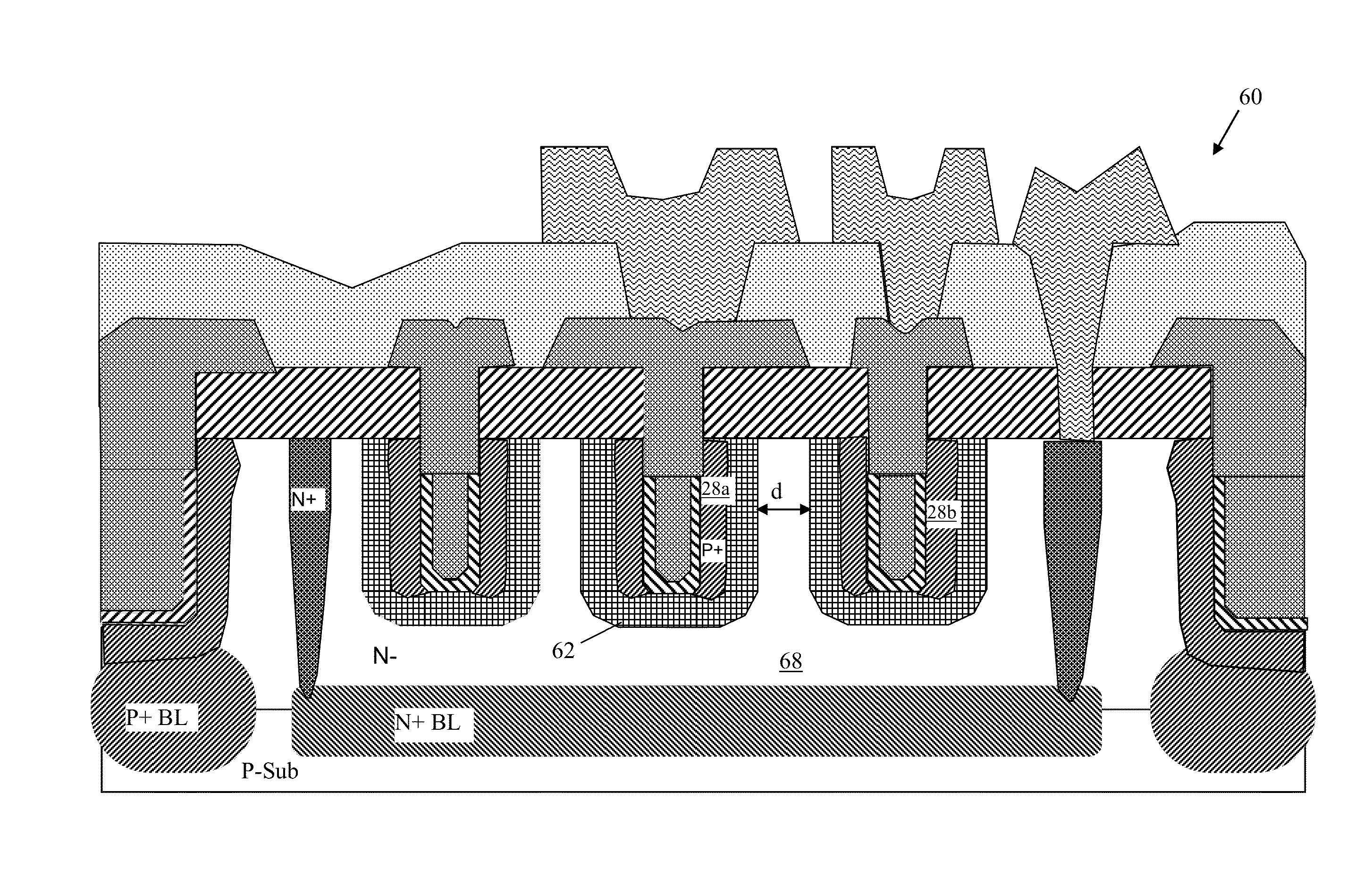
[0025]In the present invention, the trench emitter and trench collector are formed by ion implantation into the sidewall of trenches formed in a semiconductor layer. A bottom portion of the trench is lined with a thin sidewall oxide layer with the remaining portion filled with polysilicon. The thin sidewall oxide layer at the bottom portion of the trenches has the effect of preventing emitter-to-base breakdown at the bottom corners of the trenches.
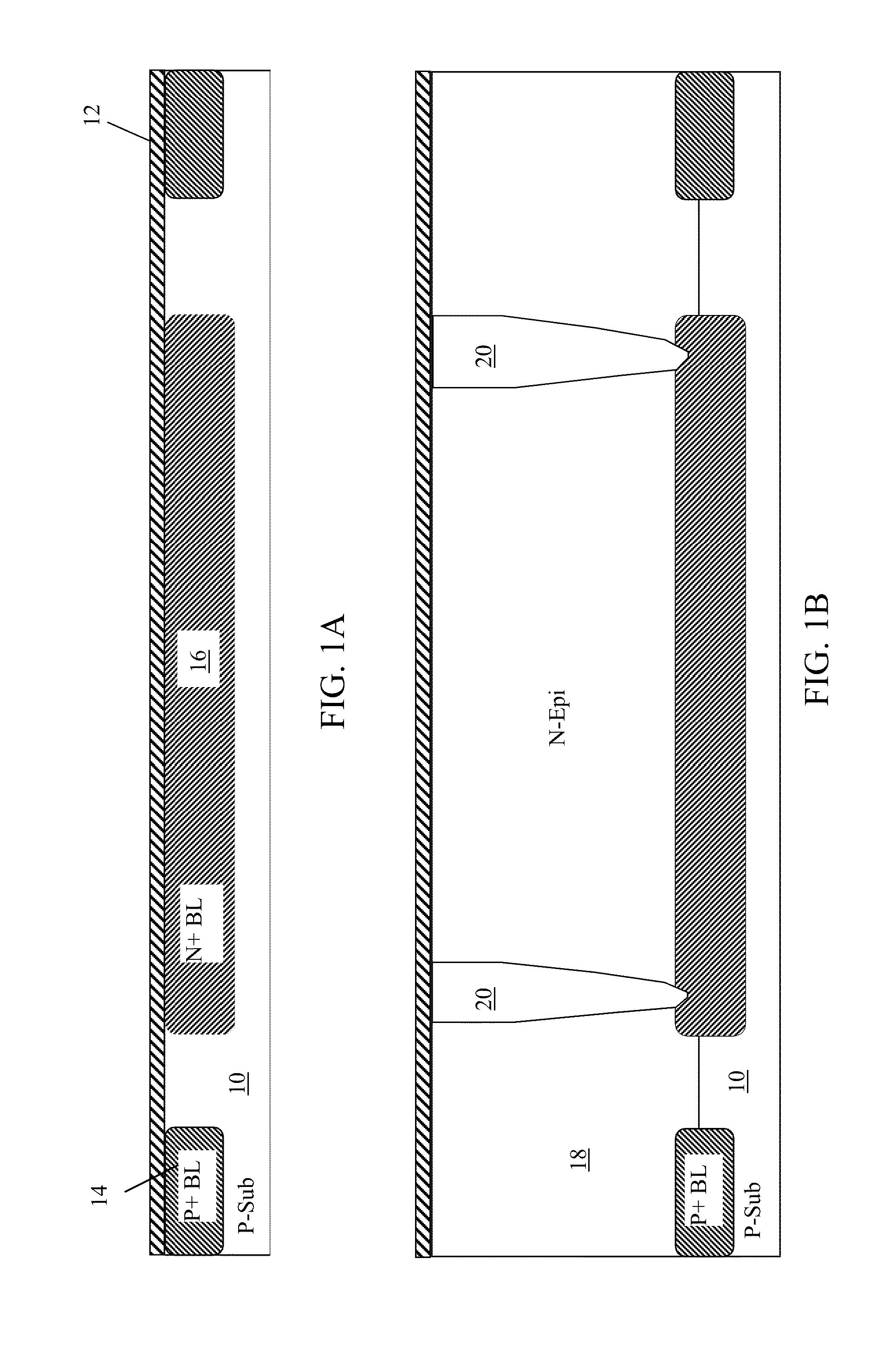
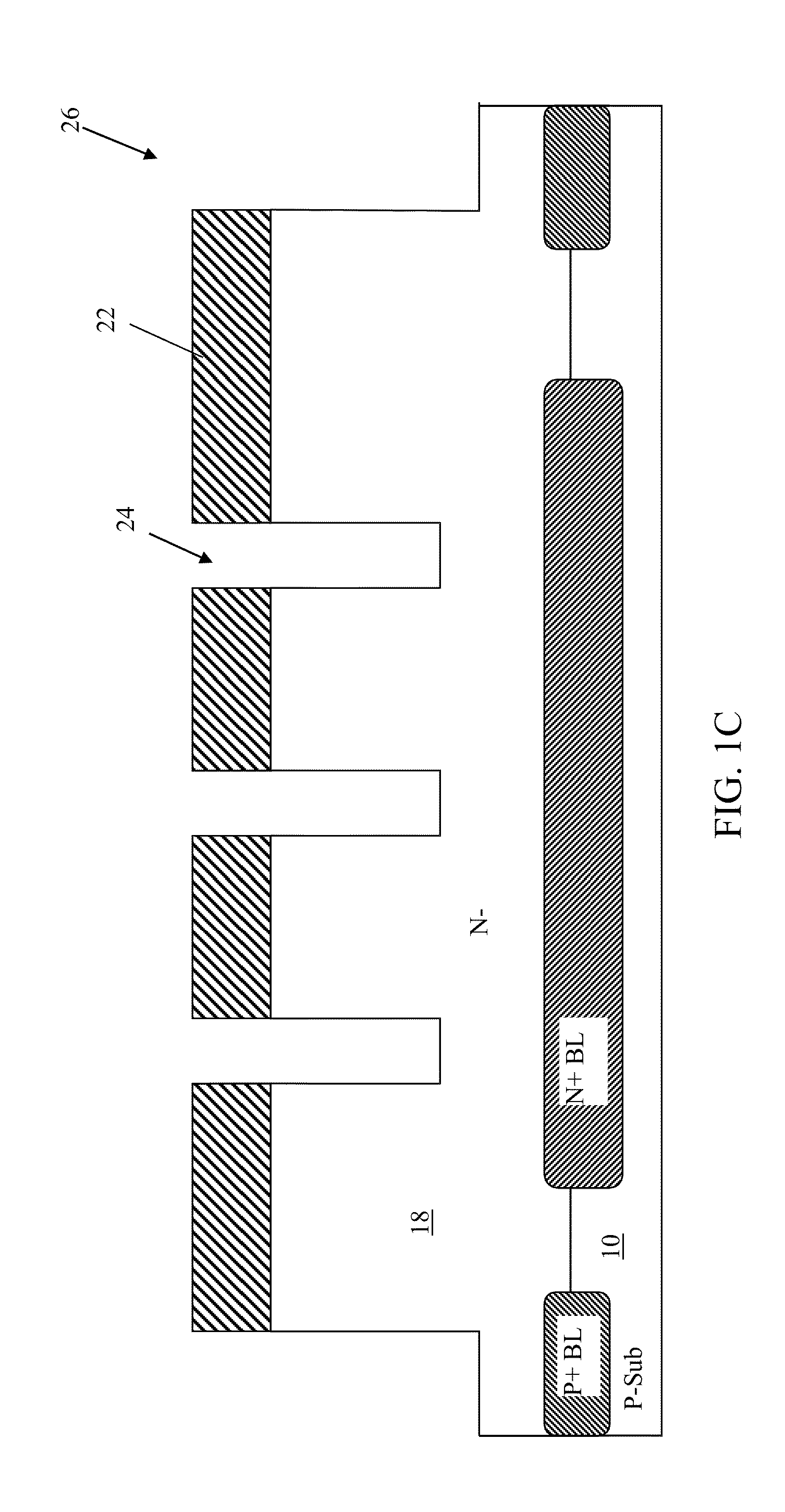
[0026]The fabrication process and the structure of the lateral PNP transistor of the present invention will now be described with reference to FIGS. 1A to 1K. Referring to FIGS. 1A to 1K, the lateral PNP transistor is formed on a P-type silicon substrate 10. A buffer oxide layer 12 may be formed on the top surface of the substrate 10 before the ion implantation steps that follow to form P+ buried layer 14 and N+ buried layer 16. The P+ buried layer 14 and the N+ buried layer 16 are formed using separate masking and ion implantation steps. ...
second embodiment
[0045]In the present invention, the trench emitter and trench collector are formed by filling trenches formed in a semiconductor layer with heavily doped polysilicon layer and auto-doping the trench sidewalls by out-diffusion of dopants from the doped polysilicon filler. An oxide layer is formed on the bottom portion of the trenches prior to polysilicon deposition. The oxide layer provides insulation and prevents emitter to base breakdown at the bottom corners of the trenches.
[0046]The fabrication process and the structure of the lateral PNP transistor of the present invention will now be described with reference to FIGS. 5A to 5J. Referring to FIGS. 5A to 5J, the lateral PNP transistor is formed on a P-type silicon substrate 10. A buffer oxide layer 12 may be formed on the top surface of the substrate 10 before the ion implantation steps that follow to form P+ buried layer 14 and N+ buried layer 16. The P+ buried layer 14 and the N+ buried layer 16 are formed using separate masking...
PUM
 Abstract
Description
Claims
Application Information


