Semiconductor process

a technology of semiconductor structure and process, applied in the direction of semiconductor devices, basic electric elements, electrical equipment, etc., can solve the problem of reducing the electrical performance of the semiconductor structure formed on the fin-shaped structur

Active Publication Date: 2013-03-28
UNITED MICROELECTRONICS CORP
View PDF0 Cites 15 Cited by
  • Summary
  • Abstract
  • Description
  • Claims
  • Application Information

AI Technical Summary

Benefits of technology

[0010]The present invention provides a semiconductor process, which forms a melting layer on the sidewalls of the fin-shaped structure by a thermal treatment process (especially to a thermal treatment process with a temperature higher than 1200° C.). In doing this,...

Problems solved by technology

However, the surfaces of the sidewalls of the fin-shaped structure formed by the lithography process are unsmooth and have defects formed as etching causes a bad quality of the chan...

Method used


Image

  • Semiconductor process
  • Semiconductor process
  • Semiconductor process

Examples


Embodiment Construction

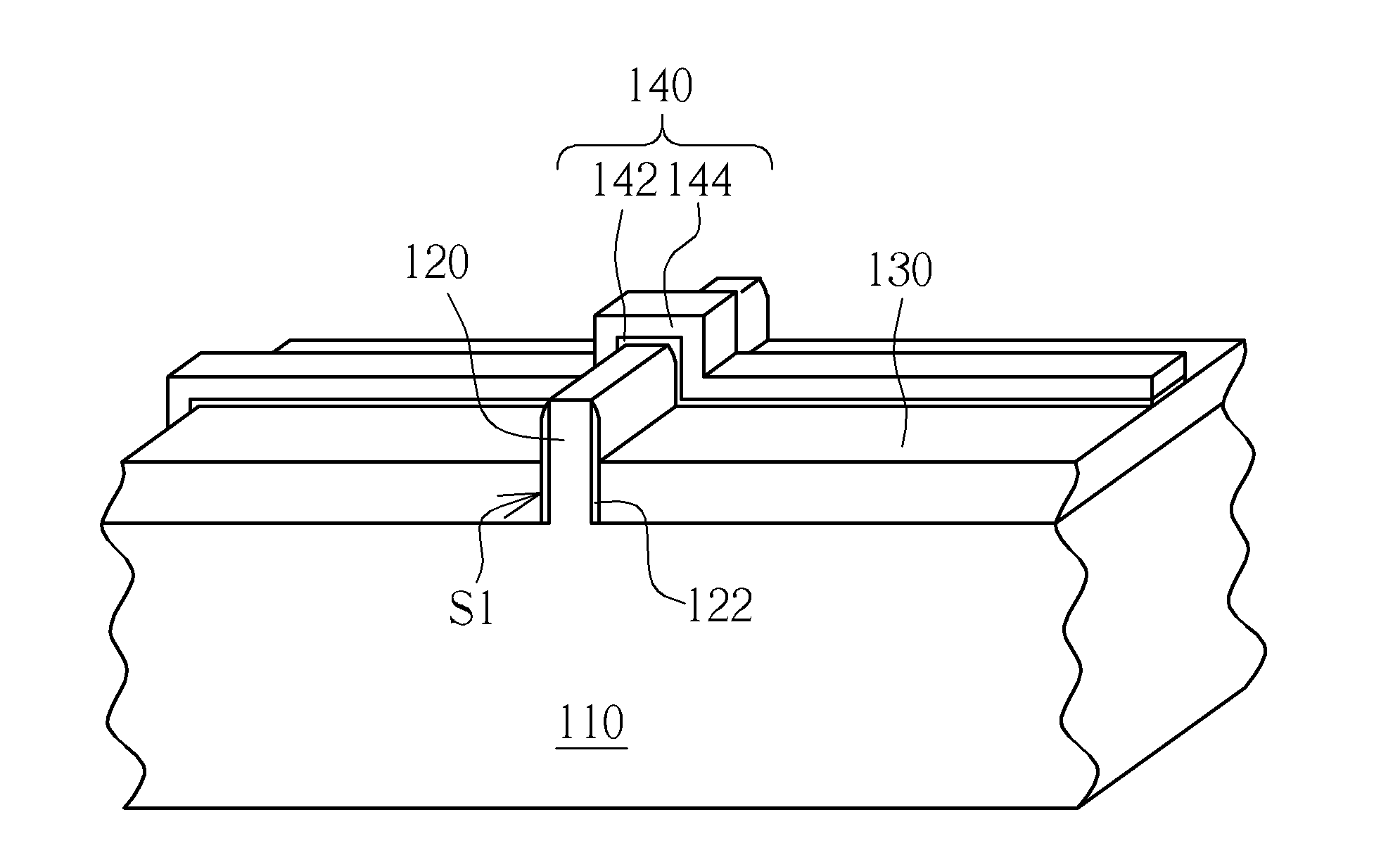
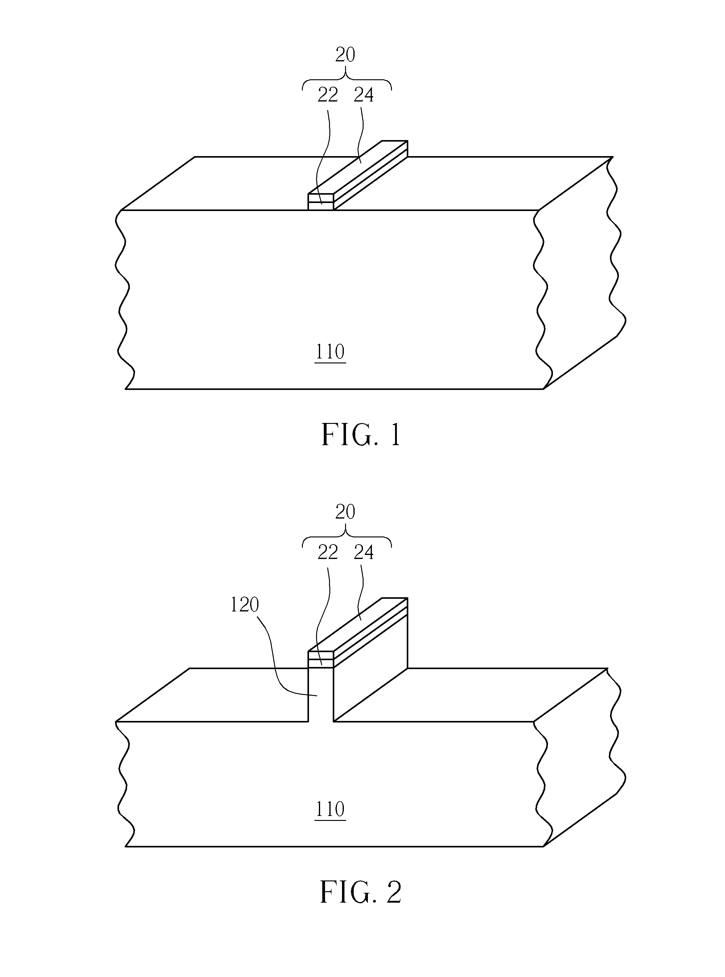
[0015]FIGS. 1-10 schematically depict a cross-sectional view of a semiconductor process according to one preferred embodiment of the present invention. As shown in FIG. 1, a substrate 110 is provided, wherein the substrate 110 may be a semiconductor substrate such as a silicon substrate, a silicon containing substrate, a III-V group-on-silicon (such as GaN-on-silicon) substrate, a graphene-on-silicon substrate or a silicon-on-insulator (SOI) substrate. A mask layer 20 is formed on the substrate 110, wherein the mask layer 20 may include a pad oxide layer 22 and a nitride layer 24 located on the pad oxide layer 22. A lithography process is performed to pattern the mask layer 20 and expose a part of the substrate 110.

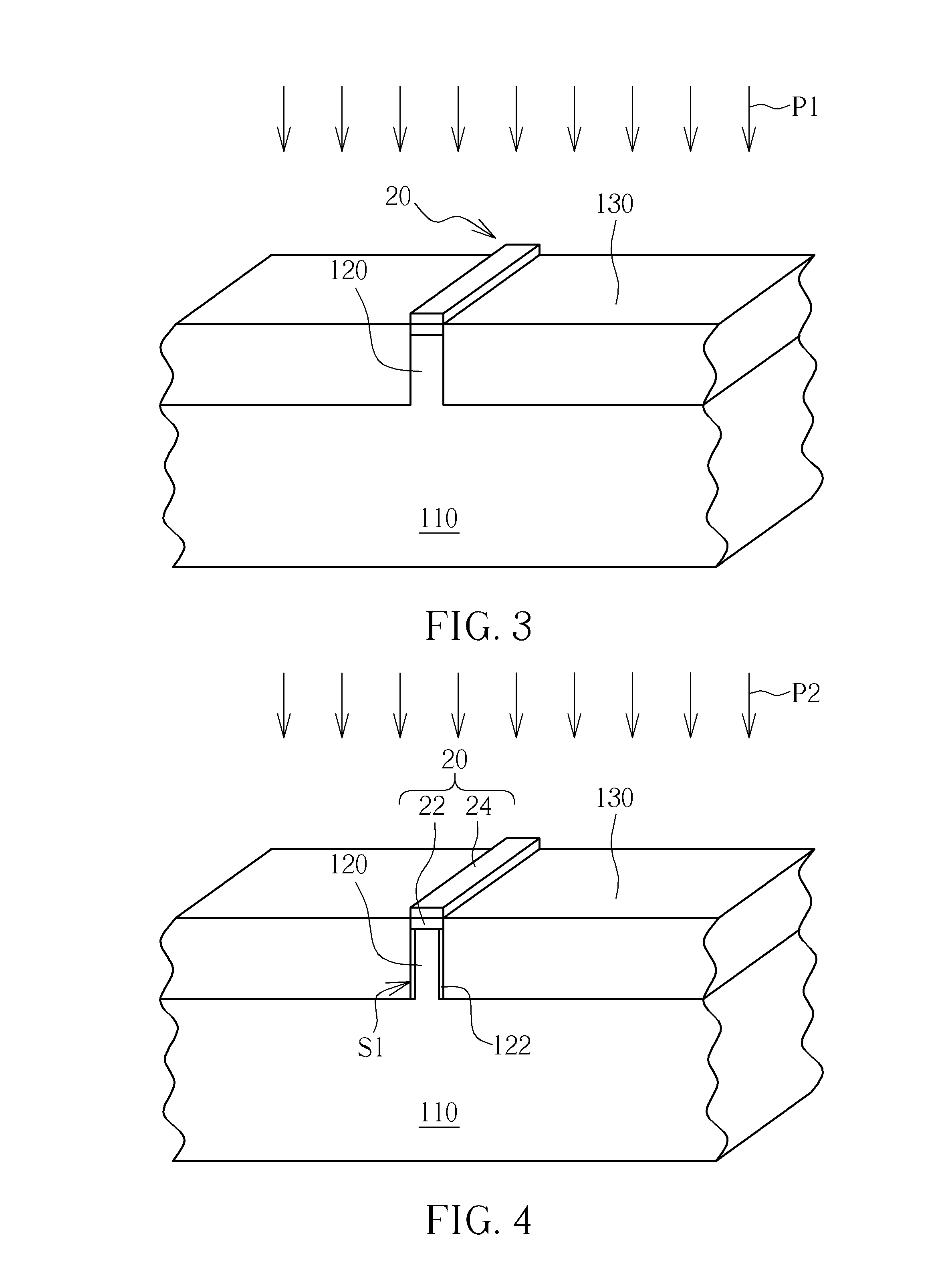
[0016]As shown in FIG. 2, the substrate 110 is etched and then a fin-shaped structure 120 is formed by using the mask layer 20 as a hard mask. In another embodiment, the mask layer 20 is patterned to expose the region of the substrate 110 needed to form a fin-shaped struc...


PUM


Abstract

A semiconductor process includes the following steps. A substrate is provided. At least a fin-shaped structure is formed on the substrate and an oxide layer is formed on the substrate without the fin-shaped structure forming thereon. A thermal treatment process is performed to form a melting layer on at least a part of the sidewall of the fin-shaped structure.

Description

BACKGROUND OF THE INVENTION[0001]1. Field of the Invention[0002]The present invention relates generally to a semiconductor process, and more specifically, to a semiconductor process, which applies a thermal treatment process to make the sidewalls of fin-shaped structures smoother.[0003]2. Description of the Prior Art[0004]With increasing miniaturization of semiconductor devices, various Fin-shaped field effect transistor (FinFET) devices have been developed. The Fin-shaped field effect transistor (FinFET) is advantageous for the following reasons. First, manufacturing processes of Fin-shaped field effect transistor (FinFET) devices can be integrated into traditional logic device processes, and thus are more compatible. In addition, since the three-dimensional structure of the FinFET increases the overlapping area between the gate and the substrate, the channel region is controlled more effectively. This therefore reduces drain-induced barrier lowering (DIBL) effect and short channel...

Claims


Application Information

Patent Timeline
IPC IPC(8): H01L21/31
CPCH01L29/66795H01L21/3247H01L29/7854
Inventor LIN, CHIEN-LIANGTSAI, SHIH-HUNGLIN, CHUN-HSIENSUN, TE-LINWANG, SHAO-WEIYEN, YING-WEIWANG, YU-REN
Owner UNITED MICROELECTRONICS CORP
Why Eureka
Try Eureka