Optical system and apparatus for laser heat treatment and method for producing semiconductor devices by using the same

a laser heat treatment and optical system technology, applied in laser beam welding apparatus, metal working apparatus, manufacturing tools, etc., can solve the problems of poor uniformity of polycrystalline silicon thin film, difficult to incorporate an integrated circuit having the required high-speed operation and high performance to the display panel, and poor performance of thin film transistors

Inactive Publication Date: 2002-08-20
MITSUBISHI ELECTRIC CORP
View PDF11 Cites 174 Cited by
  • Summary
  • Abstract
  • Description
  • Claims
  • Application Information

AI Technical Summary

Problems solved by technology

At the present, however, since the active layer of the transistors has been made of a silicon thin film of low crystallinity, the thin film transistor has poor performance exemplified by low mobility, thus making it difficult to incorporate an integrated circuit having the required high-speed operation and high performance to the display panel.
Consequently, since the polycrystalline silicon thin film has very poor uniformity within the plane after heat treatment with a laser beam, there has been reported no attempt of producing thin film transistors with this technique.
However, the conventional optical systems used for forming linear beams do not allow selection of a proper profile in the direction of width.
Also because the beam is homogenized in two perpendicular directions, it has not been possible to converge the linear beam to an extremely small width.

Method used


Image

  • Optical system and apparatus for laser heat treatment and method for producing semiconductor devices by using the same
  • Optical system and apparatus for laser heat treatment and method for producing semiconductor devices by using the same
  • Optical system and apparatus for laser heat treatment and method for producing semiconductor devices by using the same

Examples


embodiment 1

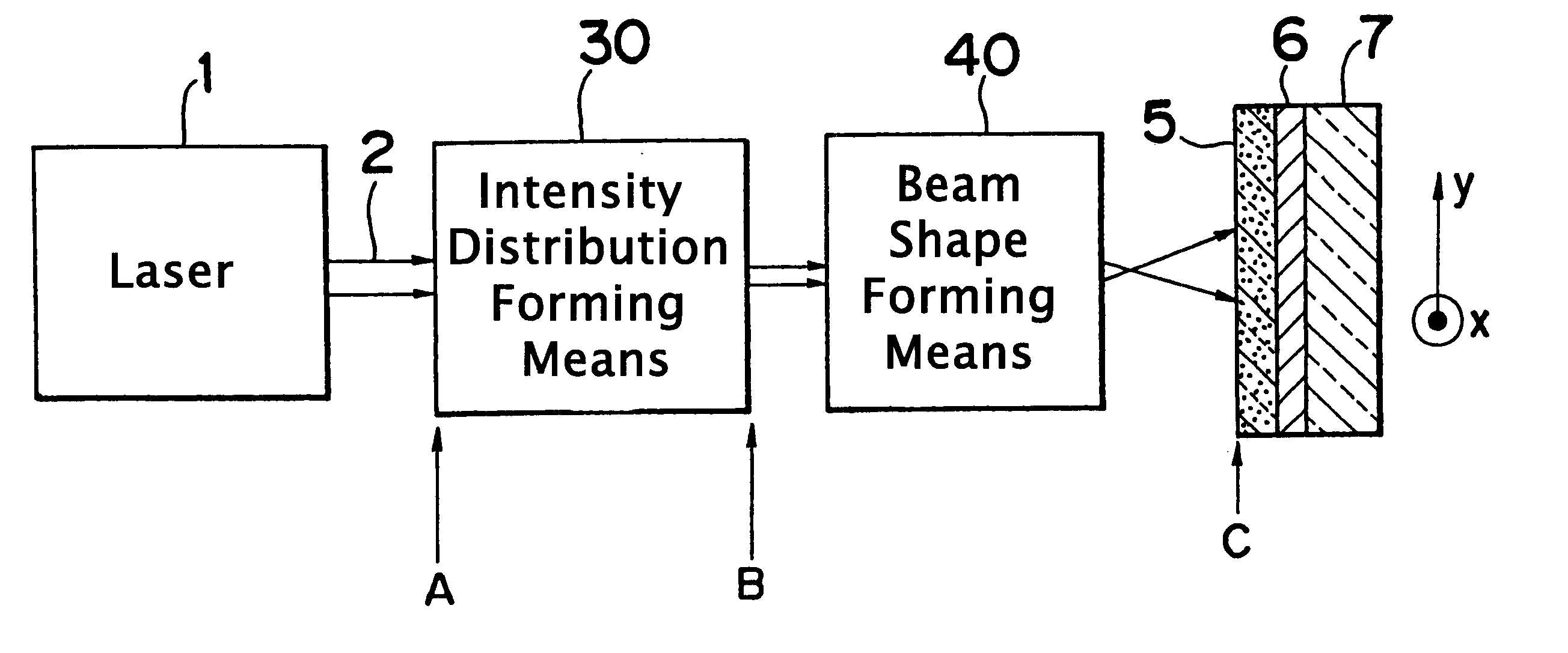
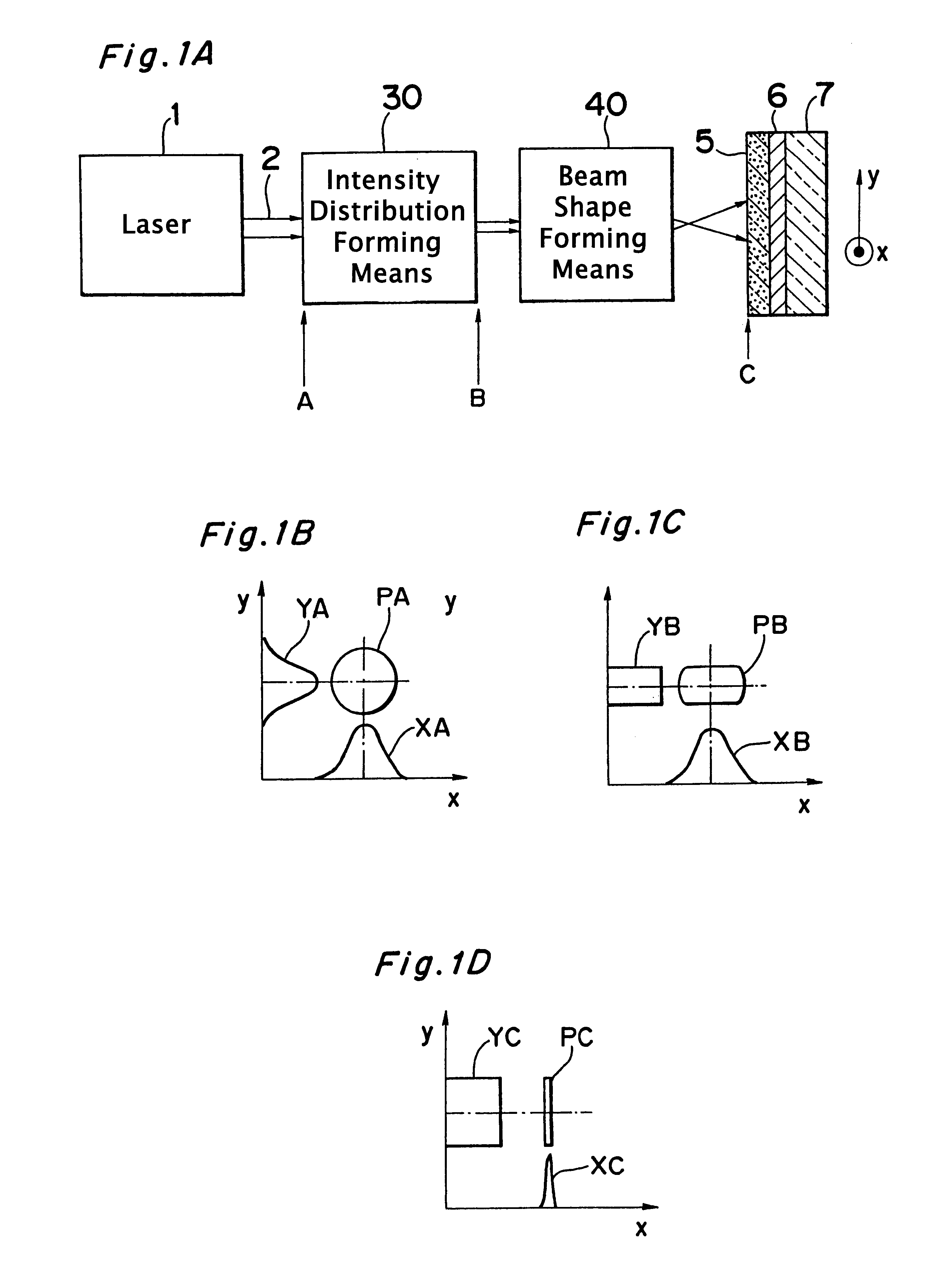
FIGS. 3A and 3B show an optical system for laser heat treatment of an embodiment of the present invention, wherein an intensity distribution forming means 30 comprises a light transmitting element or waveguide that has totally reflecting planes. The intensity distribution forming means 30 may employ a light transmitting element with a pair of reflecting planes opposite to each other, for example, a wedge-shaped transparent element 31 made of a light transmitting material. Another light transmitting element or lightguide may use a pair of tapered or parallel mirrors opposed to each other with a distance slightly narrower than a diameter of the primary laser beam.

Description shows an example of using the wedge-shaped transparent element 31. The wedge-shaped element 31 is a tapered transparent block formed in the shape of a wedge, with the dimension in y direction decreasing toward the tip as shown in FIG. 3A, and the reflecting planes are separated at a distance slightly narrower than...

embodiment 2

In this embodiment shown in FIGS. 4A and 4B, the intensity distribution forming means employs a condenser lens 32 and a waveguide 33 consisting of a pair of reflecting planes disposed to oppose each other in front of the lens 32.

The waveguide 33 may comprise a light transmitting block having two totally reflecting planes opposed to each other, or a pair of mirrors opposed to each other.

For the condenser lens 32 which focuses the laser beam emitted by the oscillator into the waveguide 33, a spherical convex lens or a cylindrical convex lens may be used to converge or diverge in y direction the light into a waveguide.

An example of the intensity distribution forming means 30 is a combination of a spherical lens used as the lens 32 and a narrow light emitting block used as the waveguide 33. In this example, a pair of wide surfaces perpendicular to y direction of the block are used as totally reflecting planes.

The laser beam 2 emitted from the laser oscillator 1 is introduced by the conv...

embodiment 3

In another embodiment, the intensity distribution forming means 30 of the optical system for laser heat treatment comprises separated cylindrical lenses 34 that consist of two semi-cylindrical lenses, which are two halves obtained by dividing a single cylindrical lens at the center thereof, spaced from each other as shown in FIGS. 5A and 5B.

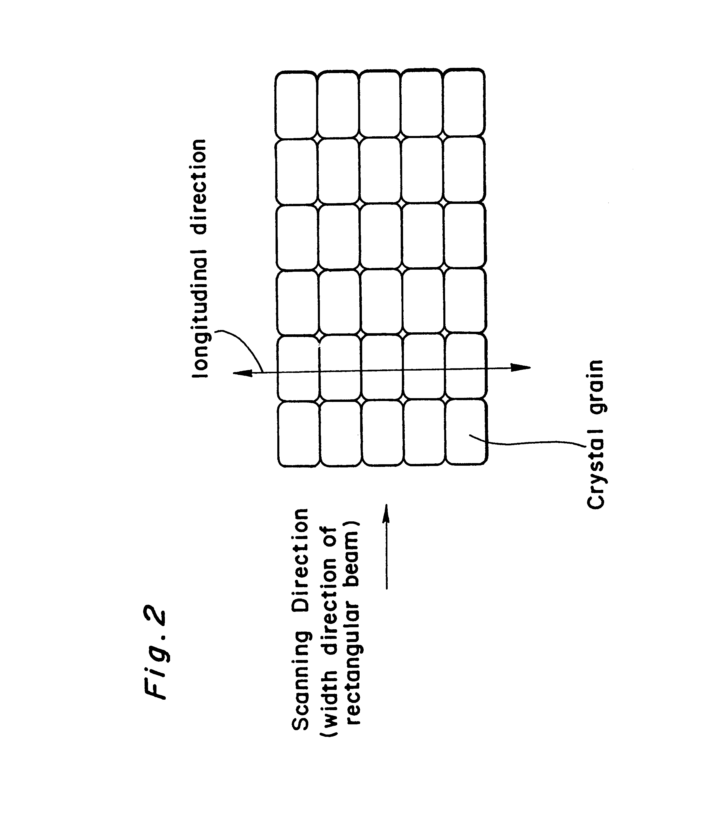
As shown in FIG. 5A, the separated cylindrical lenses 34 and 34 separated along y direction are disposed with the longitudinal direction thereof being disposed in x direction. The laser beam 2 emitted by the laser oscillator 1 is separated into a peripheral radiant fluxes refracted by the semi-cylindrical lenses and a middle radiant flux that passes straight between the two semi-cylindrical lenses. The separated radiant fluxes are combined with the middle radiant flux at the entrance of the beam shape forming means 40 to form a substantially uniform intensity distribution. In x direction, on the other hand, the laser beam 2 is output while mainta...


PUM

PropertyMeasurementUnit
wavelengthaaaaaaaaaa

Abstract

An optical system that controls laser beam spot profile for forming a high performance thin film by a laser heat treatment process is provided. In the optical system that irradiates a rectangular laser beam on a film formed on a substrate, intensity distribution forming, apparatus makes the intensity distribution uniform in the longitudinal direction while maintaining the properties of the laser beam 2 such as directivity in the direction of shorter side, making it possible to concentrate the light to a limit permitted by the nature of the laser beam and achieve the maximum intensity gradient on the film disposed on the substrate. Thus a steep temperature distribution can be generated on the film disposed on the substrate and, as a result, high performance thin film can be formed.

Description

1. Field of the InventionThe present invention relates to an optical system and apparatus for laser heat treatment, and to a method for producing semiconductor devices by laser crystallization by heat-treating a thin silicon thin film formed on a substrate to convert an amorphous or polycrystalline silicon thin film into coarse-grained silicon.2. Prior ArtThe pixel section of a liquid crystal display panel is constituted from thin film switching transistors formed from an amorphous or polycrystalline silicon thin film on a substrate of glass or synthesized quartz. A driver circuit for driving the pixel transistors has been arranged mostly outside the panel, but if such a driver circuit were formed together in the panel, tremendous advantages would be achieved in terms of reliability of the liquid crystal panel with lowered cost of production.At the present, however, since the active layer of the transistors has been made of a silicon thin film of low crystallinity, the thin film tra...

Claims


Application Information

Patent Timeline
Patent Type & Authority Patents(United States)
IPC IPC(8): B23K26/06B23K26/073H01L21/20H01L21/02H01L21/268H01L21/324
CPCB23K26/0732B23K2201/40H01L21/2026B23K2101/40H01L21/02686H01L21/0242H01L21/02691H01L21/02488H01L21/02422H01L21/02678H01L21/02532H01L21/324H01L21/02675
Inventor OKAMOTO, TATSUKIOGAWA, TETSUYAFURUTA, KEISUKETOKIOKA, HIDETADASASAGAWA, TOMOHIRONISHIMAE, JUNICHIINOUE, MITSUOSATO, YUKIO
Owner MITSUBISHI ELECTRIC CORP
Why Eureka
Try Eureka