Multilayer ceramic capacitor and method for manufacturing the same

a multi-layer ceramic and capacitor technology, applied in the direction of fixed capacitors, stacked capacitors, fixed capacitor details, etc., can solve the problems of soldering defects, impossible recalling defective products,

Inactive Publication Date: 2013-04-11
SAMSUNG ELECTRO MECHANICS CO LTD
View PDF1 Cites 32 Cited by
  • Summary
  • Abstract
  • Description
  • Claims
  • Application Information

AI Technical Summary

Benefits of technology

[0009]An object of the present invention is to provide a multilayer ceramic capacitor having a uniform nickel plating layer without nickel non-plating defects, which can be formed even though nickel electroplating is performed on a surface of an external electrode, and having a structure not causing soldering defects at the time of mounting.

Problems solved by technology

Furthermore, since an MLCC for an electronic product becomes smaller, work for recalling defective products is impossible, and as a result, a high-reliability product is requested, like in an MLCC for an electrical device.
However, in a case of the Ag-epoxy external electrode, epoxy having no conductivity is largely exposed to the surface thereof, which causes soldering defects due to non-plating defects at the time of mounting, in a case where a current nickel electroplating process is performed (See, FIGS. 1 and 2).

Method used


Image

  • Multilayer ceramic capacitor and method for manufacturing the same
  • Multilayer ceramic capacitor and method for manufacturing the same
  • Multilayer ceramic capacitor and method for manufacturing the same

Examples


example 1

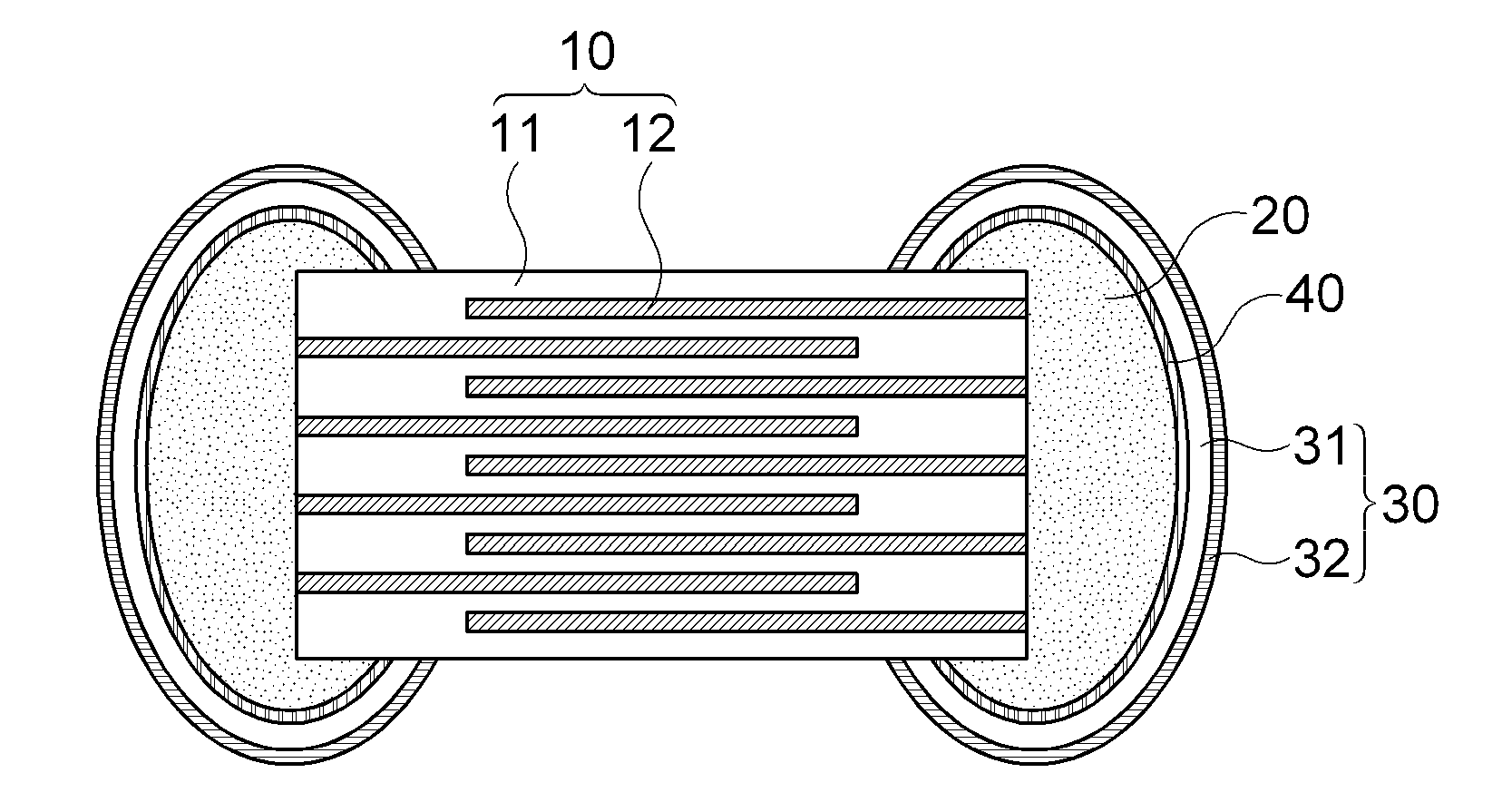
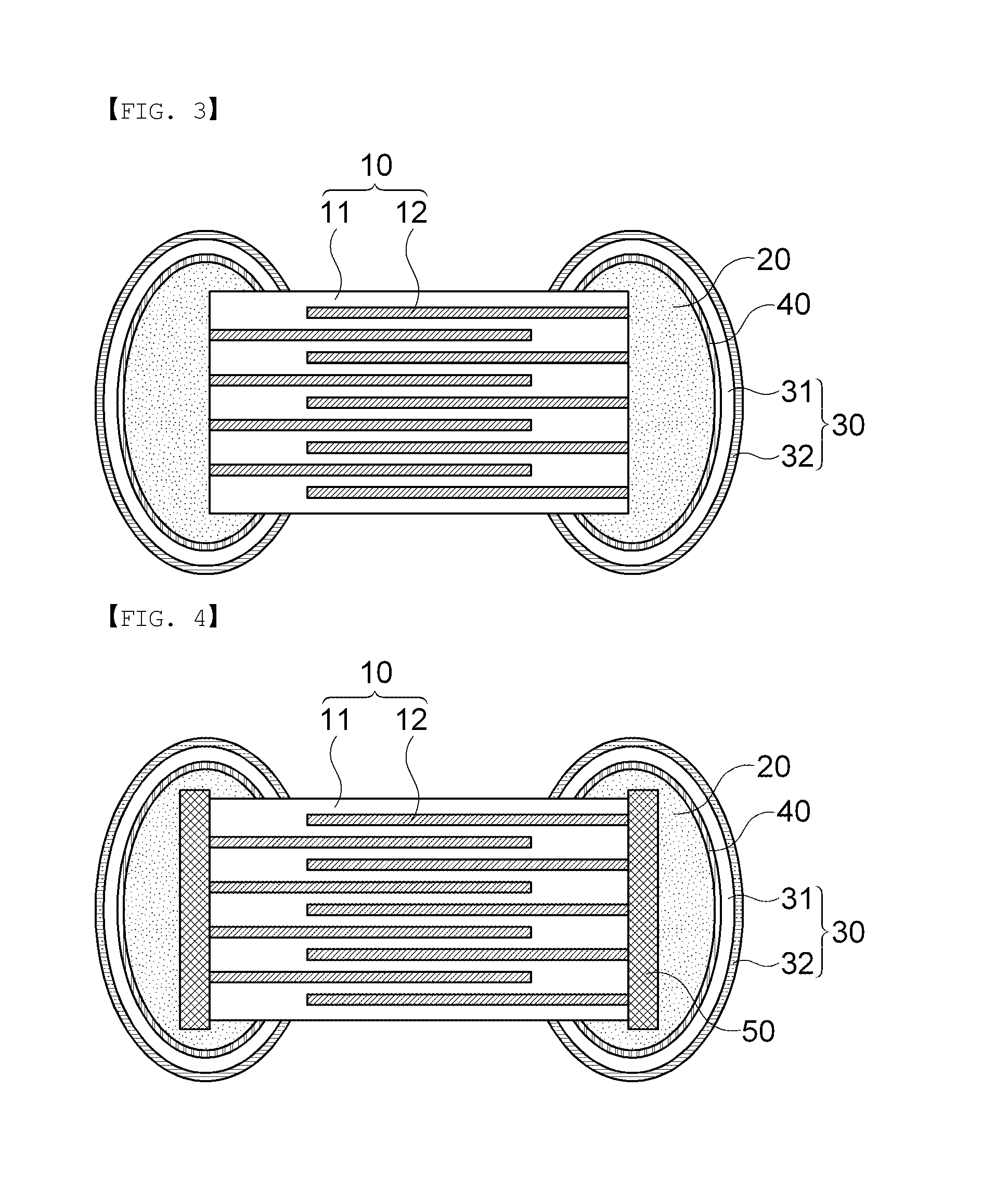
[0058]Conductive inner electrodes were respectively printed on dielectric layers prepared by using slurry including a dielectric material. Then, the printed dielectric layers were laminated in a predetermined thickness, to manufacture a capacitor main body, which was then fired.

[0059]External electrodes (Ag-epoxy) for electric connection with inner electrodes are coated and hardened / fired on both lateral surfaces of the capacitor main body.

[0060]Then, electroless reduction tin (Sn) plating layers with a thickness of 1 μm were formed on the external electrodes. Ni electroplating layers and electroless Sn plating layers were formed on the electroless reduction tin (Sn) plating layers.

experimental example 1

[0061]After the electroless reduction tin plating layers of the manufactured multilayer ceramic capacitor was introduced, the number of soldering defects was checked over five times, and the results were tabulated in Table 1. A test picture showing whether or not the soldering defects are present or absent is shown in FIG. 5.

TABLE 1FirstSecondThirdFourthFifthNumber of soldering0 / 16000 / 16000 / 16000 / 16000 / 1600defects

[0062]As shown in Table 1, it was confirmed from the results of measuring the number of soldering defects five times that soldering defects were never generated. From these results, it can be seen that the soldering defect problem occurring due to nickel non-plating can be completely solved by forming the electroless plating layer on the external electrode before nickel and tin plating layers are formed. In addition, these results confirmed that nickel plating was more effective when the electroless plating layer is formed on the external electrode and then the nickel plati...


PUM

PropertyMeasurementUnit
thicknessaaaaaaaaaa
thicknessaaaaaaaaaa
thicknessaaaaaaaaaa

Abstract

Disclosed herein are a multilayer ceramic capacitor and a method for manufacturing the same. The multilayer ceramic capacitor includes: a capacitor main body having dielectric layers and inner electrodes laminated therein; external electrodes and plating layers formed on a surface of the capacitor main body; and electroless plating layers formed between the external electrodes and the plating layers.According to the examples of the present invention, the electroless plating layer is formed before the plating layer is formed on the external electrode, thereby solving non-plating problems when the plating layer made of nickel or the like is formed on the external electrode. Therefore, soldering defects due to nickel non-plating or the like can be solved at the time of mounting, and thus, a multilayer ceramic capacitor having high reliability can be provided.

Description

CROSS REFERENCE(S) TO RELATED APPLICATIONS[0001]This application claims the benefit under 35 U.S.C. Section 119 of Korean Patent Application Serial No. 10-2011-0101910, entitled “Multilayer Ceramic Capacitor and Method for Manufacturing the Same” filed on Oct. 6, 2011, which is hereby incorporated by reference in its entirety into this application.BACKGROUND OF THE INVENTION[0002]1. Technical Field[0003]The present invention relates to a multilayer ceramic capacitor and a method for manufacturing the same.[0004]2. Description of the Related Art[0005]Following the trend that a semiconductor device has a small size and high speed / high frequency, a super high-capacity multilayer ceramic capacitor (MLCC) is requested. For this, a ratio of capacitance over size needs to be increased, and thus, a dielectric layer and an inner electrode layer need to be further thinned.[0006]Therefore, crystal particles constituting the dielectric layer are requested to have material properties such as sma...

Claims


Application Information

Patent Timeline
Patent Type & Authority Applications(United States)
IPC IPC(8): H01G4/252B05D5/12
CPCH01G4/2325H01G4/30H01G4/12
Inventor YANG, JIN HYUCKKIM, YONG SEOK
Owner SAMSUNG ELECTRO MECHANICS CO LTD
Why Eureka
Try Eureka