Encapsulating sheet and optical semiconductor element device

a technology of optical semiconductor elements and encapsulating sheets, which is applied in semiconductor devices, solid-state devices, electrical devices, etc., can solve the problems of insufficient light transmittance of encapsulating sheets to meet the above-described requirements, and achieve excellent light transmission characteristics, prevent bleeding, and suppress brightness loss in encapsulating sheets.

Inactive Publication Date: 2013-04-18
NITTO DENKO CORP
View PDF6 Cites 6 Cited by
  • Summary
  • Abstract
  • Description
  • Claims
  • Application Information

AI Technical Summary

Benefits of technology

[0015]In the encapsulating sheet of the present invention, the encapsulating resin composition contains the silicone microparticles, so that the light transmission characteristics thereof is excellent, compared to the case where another additive is contained.
[0016]Therefore, in the optical semiconductor element device of the present invention provided with the optical semiconductor element which is encapsulated by the encapsulating sheet of the present invention, the brightness loss in the encapsulating sheet can be sufficiently suppressed.
[0017]In the encapsulating sheet of the present invention, the encapsulating resin composition contains the silicone microparticles at a specific proportion, so that in the optical semiconductor element device of the present invention, a bleeding can be prevented and a damage of the optical semiconductor element can be also prevented.
[0018]As a result, the optical semiconductor element device of the present invention has an excellent reliability, while having an excellent extraction efficiency of the light from the optical semiconductor.

Problems solved by technology

However, in the optical semiconductor encapsulating material in a sheet shape described in Japanese Unexamined Patent Publication No. 2011-228525, the light transmittance thereof is insufficient to satisfy the above-described requirement.

Method used


Image

  • Encapsulating sheet and optical semiconductor element device
  • Encapsulating sheet and optical semiconductor element device
  • Encapsulating sheet and optical semiconductor element device

Examples


prepared example 1

[0504]

[0505]15.76 g (0.106 mol) of a vinyltrimethoxysilane (an ethylenic silicon compound) and 2.80 g (0.0118 mol) of a (3-glycidoxypropyl)trimethoxysilane (a silicon compound containing an epoxy group) were blended into 2031 g (0.177 mol) of a polydimethylsiloxane containing silanol groups at both ends (a polysiloxane containing silanol groups at both ends, in general formula (1), all of R1s are methyl, the average of “z” is 155, a number average molecular weight of 11500, a silanol group equivalent of 0.174 mmol / g), which was heated at 40° C., and the obtained mixture was stirred and mixed.

[0506]The molar ratio (the number of moles of SiOH group / the total number of moles of SiOCH3 group) of the SiOH group in the polydimethylsiloxane containing silanol groups at both ends to the SiOCH3 group in the vinyltrimethoxysilane and (3-glycidoxypropyl)trimethoxysilane was 1 / 1.

[0507]After the stirring and mixing, 0.97 mL (0.766 g, a catalyst content: 0.88 mmol, corresponding to 0.50 mol with...

example 1

[0511]

[0512]8 g of YAG:Ce (a phosphor, an average particle size of 8.9 μm) and 20 g of Tospearl 2000B (trade name, polymethylsilsesquioxane microparticles, an average particle size of 6.0 μm, manufactured by Momentive Performance Materials Inc.) were added to 72 g of the above-described silicone resin composition to be stirred at room temperature (at 20° C.) for 1 hour. After the stirring, the obtained mixture was subjected to a defoaming process under a reduced pressure with a vacuum dryer at room temperature for 30 minutes or more.

[0513]In this way, an encapsulating resin composition was prepared.

[0514]

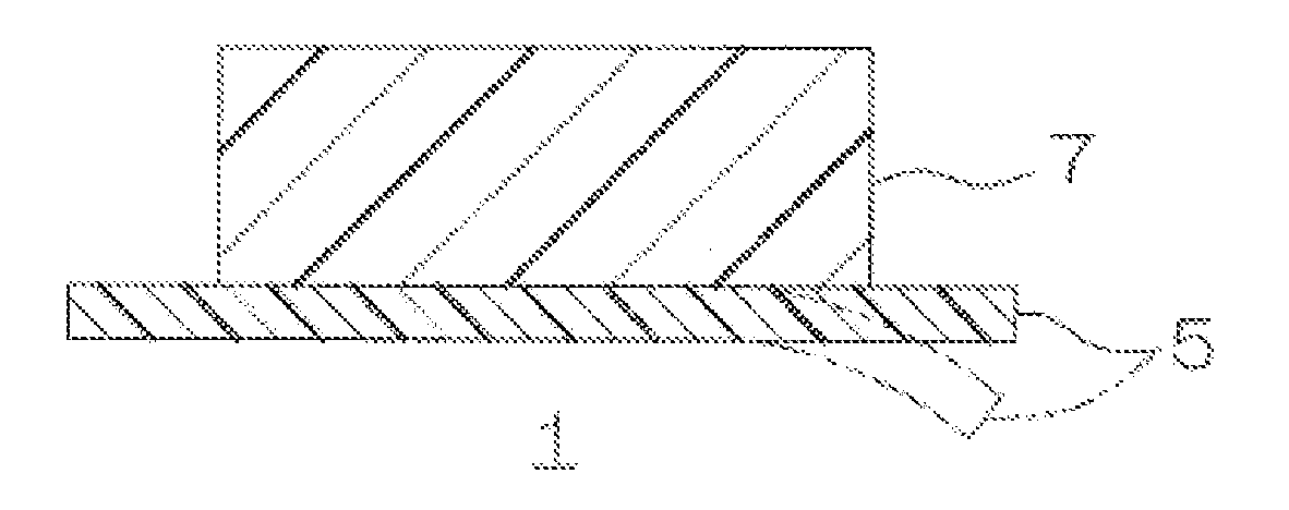
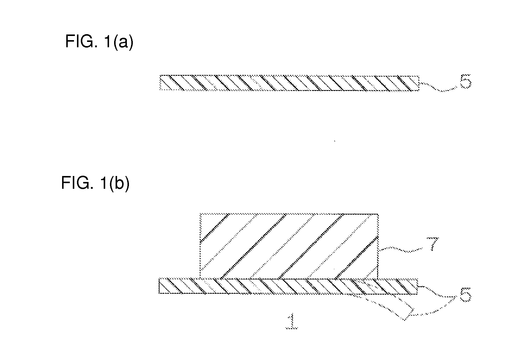
[0515]The encapsulating resin composition was applied to the upper surface of a release sheet (ref: FIG. 1(a)) made of a polyester film (trade name: SS4C, manufactured by Nippa CO., LTD., a thickness of 50 μm) with a thickness of 600 μm to be heated at 135° C. for 3 minutes, so that an encapsulating sheet in which an encapsulating resin layer having a thickness of 600 μm was laminat...


PUM

PropertyMeasurementUnit
thicknessaaaaaaaaaa
thicknessaaaaaaaaaa
mixing ratioaaaaaaaaaa

Abstract

An encapsulating sheet is formed from an encapsulating resin composition which contains an encapsulating resin and silicone microparticles, and the mixing ratio of the silicone microparticles with respect to the encapsulating resin composition is 20 to 50 mass %.

Description

CROSS-REFERENCE TO RELATED APPLICATION[0001]The present application claims priority from Japanese Patent Applications No. 2011-228921 filed on Oct. 18, 2011 and No. 2011-289901 filed on Dec. 28, 2011, the contents of which are hereby incorporated by reference into this application.BACKGROUND OF THE INVENTION[0002]1. Field of the Invention[0003]The present invention relates to an encapsulating sheet and an optical semiconductor element device, to be specific, to an optical semiconductor element device used for an optical application and an encapsulating sheet used therein.[0004]2. Description of Related Art[0005]Conventionally, a light emitting device capable of emitting high-energy light has been known.[0006]The light emitting device includes, for example, an optical semiconductor, a board mounted with the optical semiconductor, and an encapsulating material formed on the board so as to encapsulate the optical semiconductor. The optical semiconductor emits light and the emitted ligh...

Claims


Application Information

Patent Timeline
Patent Type & Authority Applications(United States)
IPC IPC(8): H01L33/56
CPCC08G77/045H01L2933/005C08G77/14C08K5/5425C08K5/5435C08G77/16C08G77/20C08K5/56C08L83/04C08G77/12H01L2933/0041H01L33/56H01L33/501H01L33/54C08L83/00H01L2224/48091H01L2924/181H01L2924/00012H01L2924/00014H01L33/50H01L33/52
Inventor KONDO, TAKASHIKONO, HIROKIEBE, YUKI
Owner NITTO DENKO CORP
Why Eureka
Try Eureka