Gas-phase synthesis of wires

a wire and gas-phase technology, applied in the field of wire formation, can solve the problems of scalability of the process, and limited production cost and through-put, and achieve the effect of high ra

Inactive Publication Date: 2013-04-25
ALIGNEDBIO AB
View PDF3 Cites 20 Cited by
  • Summary
  • Abstract
  • Description
  • Claims
  • Application Information

AI Technical Summary

Benefits of technology

[0016]The catalytic seed particles can be provided as an aerosol that is mixed with the gaseous precursors prior to, or during, initiation of wire growth. Alternatively the catalytic seed particles are formed by formation from gaseous reactants that comprises at least one of the constituents of the catalytic particles, thereby enabling a self-catalyzed wire growth.
[0017]Preferably, the method of the invention comprises providing a flow of the gas that carries the catalytic seed particles and subsequently the partly or fully formed wires through one or more reactors, each reactor comprising one or more reaction zones. Thereby the catalytic seed particles and any wires formed thereon flow sequentially through one or more reaction zones, where each reaction zone contributes to the wire growth by adding material to the wire or etching the wire. This enables to provide optimum conditions for each step in the growth process.
[0021]In another aspect of the invention, the seed particles / wires are heated by means of microwaves, infrared light or other electromagnetic radiation, instead of or as a complement to the hot wall tube furnace. This allows the gas to remain more or less cold, minimizing the amount of gas-phase reactions, while allowing growth on the hot particle / wire surfaces.
[0027]Although not limited to nanowires, semiconductor nanowires produced by the method of the invention possess some advantages with respect to conventional planar processing. While there are certain limitations in semiconductor devices fabricated using planar technology, such as lattice mismatch between successive layers, nanowire formation in accordance with the invention provides greater flexibility in selection of semiconductor materials in successive segments or shells and hence greater possibility to tailor the band structure of the nanowire. Nanowires potentially also have a lower defect density than planar layers and by replacing at least portions of planar layers in semiconductor devices with nanowires, limitations with regards to defects can be diminished. Further, nanowires provide surfaces with low defect densities as templates for further epitaxial growth. As compared to substrate-based synthesis lattice mismatch between substrate and wire does not have to be considered.
[0031]One advantage of the method and apparatus in accordance with the invention is that wires can be grown at a surprisingly high rate. Growth rates may be higher than 1 μm / s, which implies a growth time of a few seconds for a typical wire of 0.4×3 μm dimension. This means that, in a continuous process in accordance with the invention the through-put is tremendous.

Problems solved by technology

For example substrate-based synthesis provides advantageous wire properties but since wires are formed in batches the scalability of the process, and thus the production cost and through-put, are limited.

Method used


Image

  • Gas-phase synthesis of wires
  • Gas-phase synthesis of wires
  • Gas-phase synthesis of wires

Examples


Embodiment Construction

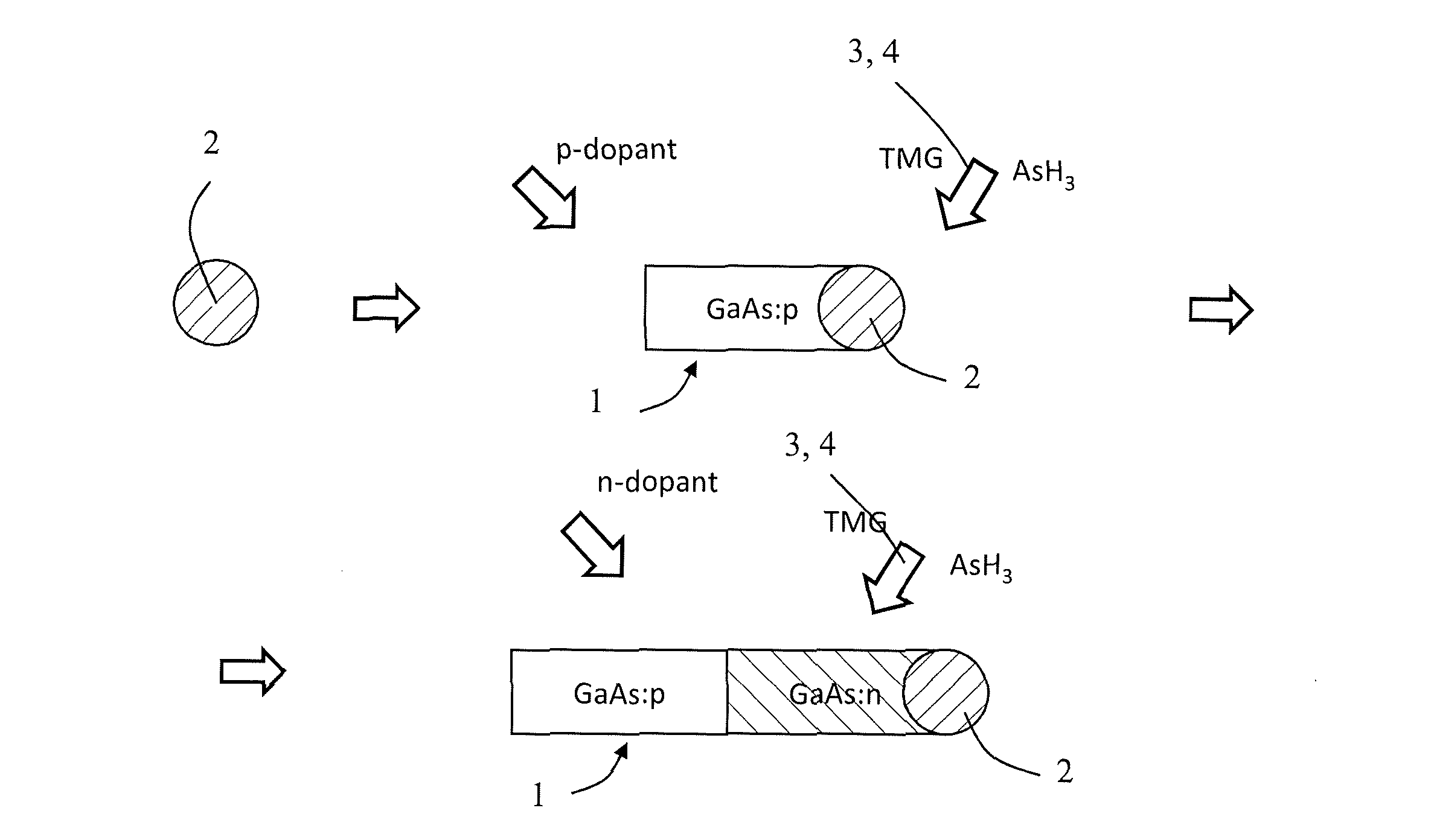
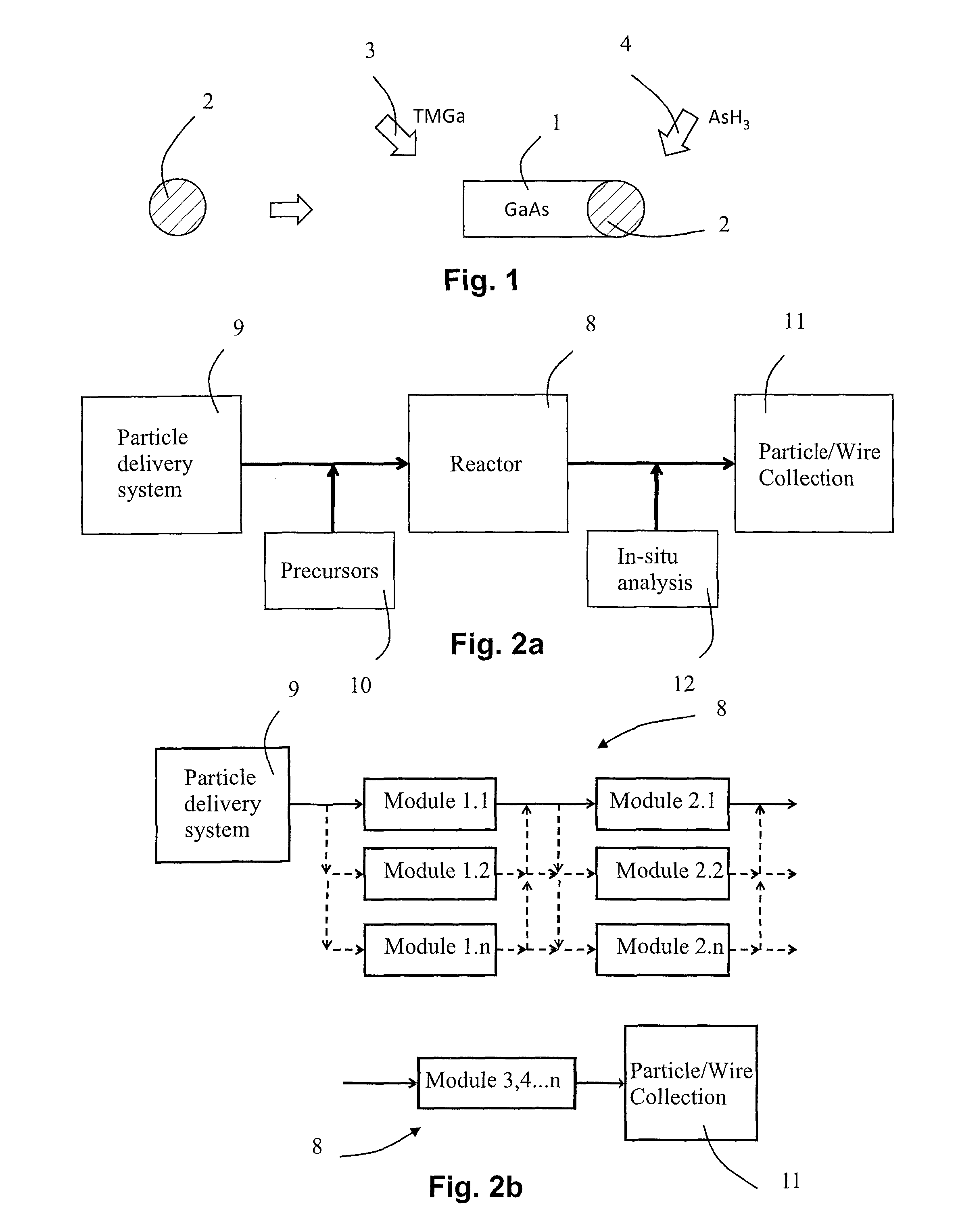
[0044]For the purpose of this application the term wire refers to an elongated object. As mentioned above, these wires may be of essentially nanometer dimensions in their width or diameter, commonly referred to as nanowires, nanowhiskers, nanorods, etc., however not limited to this.

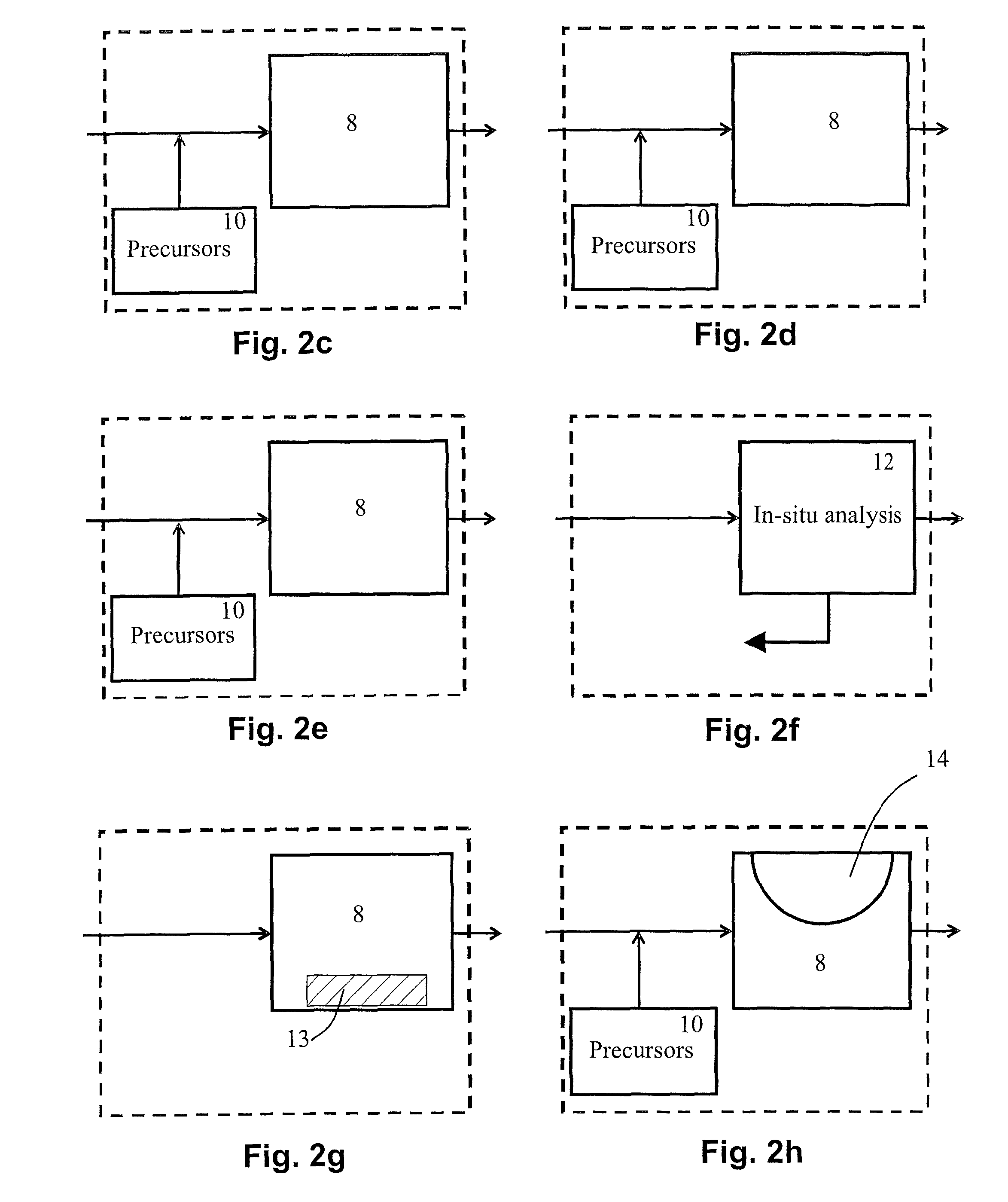
[0045]Referring to FIG. 1, basically a method for forming wires in accordance with the invention comprises[0046]providing catalytic seed particles2 suspended in a gas,[0047]providing gaseous precursors 3, 4 that comprises constituents of the wires 1 to be formed, and[0048]growing the wires 1 from the catalytic seed particles 2 in a gas-phase synthesis including the gaseous precursors 3, 4 while the catalytic seed particles are suspended in the gas.

[0049]The growth, or at least part thereof, is performed at an elevated temperature, typically in a furnace or some other kind of reactor, and starts with an initiation of the growth by catalytic decomposition of the gaseous precursors 3, 4 on the surface of the...


PUM

PropertyMeasurementUnit
temperatureaaaaaaaaaa
sizeaaaaaaaaaa

Abstract

The present invention provides a method and a system for forming wires (1) that enables a large scale process combined with a high structural complexity and material quality comparable to wires formed using substrate-based synthesis. The wires (1) are grown from catalytic seed particles (2) suspended in a gas within a reactor. Due to a modular approach wires (1) of different configuration can be formed in a continuous process. In-situ analysis to monitor and / or to sort particles and / or wires formed enables efficient process control.

Description

TECHNICAL FIELD OF THE INVENTION[0001]The present invention relates to formation of wires and in particular to gas-phase synthesis of wires in the absence of a substrate. The gas-phase synthesis is applicable to different materials, and in particular to semiconductor materials.BACKGROUND OF THE INVENTION[0002]Small elongated objects, usually referred to as nanowires, nanorods, nanowhiskers, etc. and typically comprising semiconductor materials, have up till now been synthesized using one of the following routes:[0003]liquid phase synthesis, for example by means of colloidal chemistry as exemplified US 2005 / 0054004 by Alivisatos et al,[0004]epitaxial growth from substrates, with or without catalytic particles as exemplified by the work of Samuelson et al presented in WO 2004 / 004927 A2 and WO 2007 / 10781 A1, respectively, or[0005]gas phase synthesis by means of a laser assisted catalytic growth process as exemplified by WO 2004 / 038767 A2 by Lieber et al.[0006]The properties of wires ob...

Claims


Application Information

Patent Timeline
Patent Type & Authority Applications(United States)
IPC IPC(8): C30B25/00
CPCB82Y30/00B82Y40/00C30B25/00C30B25/005C30B29/403C30B29/62C30B29/40C30B29/42C30B25/02
Inventor SAMUELSON, LARSMAGNUSSON, MARTINDEPPERT, KNUTHEURLIN, MAGNUS
Owner ALIGNEDBIO AB
Why Eureka
Try Eureka