
Opto-electrical devices incorporating metal nanowires

a technology of metal nanowires and opto-electric devices, which is applied in the direction of thermoelectric devices, sustainable manufacturing/processing, and final product manufacturing, etc., can solve the problem that not all the light generated from the organic stack is capable of being generated via the external mode, and achieve the effect of improving light out-coupling

Active Publication Date: 2013-05-02
CHAMP GREAT INTL
View PDF0 Cites 71 Cited by
  • Summary
  • Abstract
  • Description
  • Claims
  • Application Information

AI Technical Summary

Benefits of technology

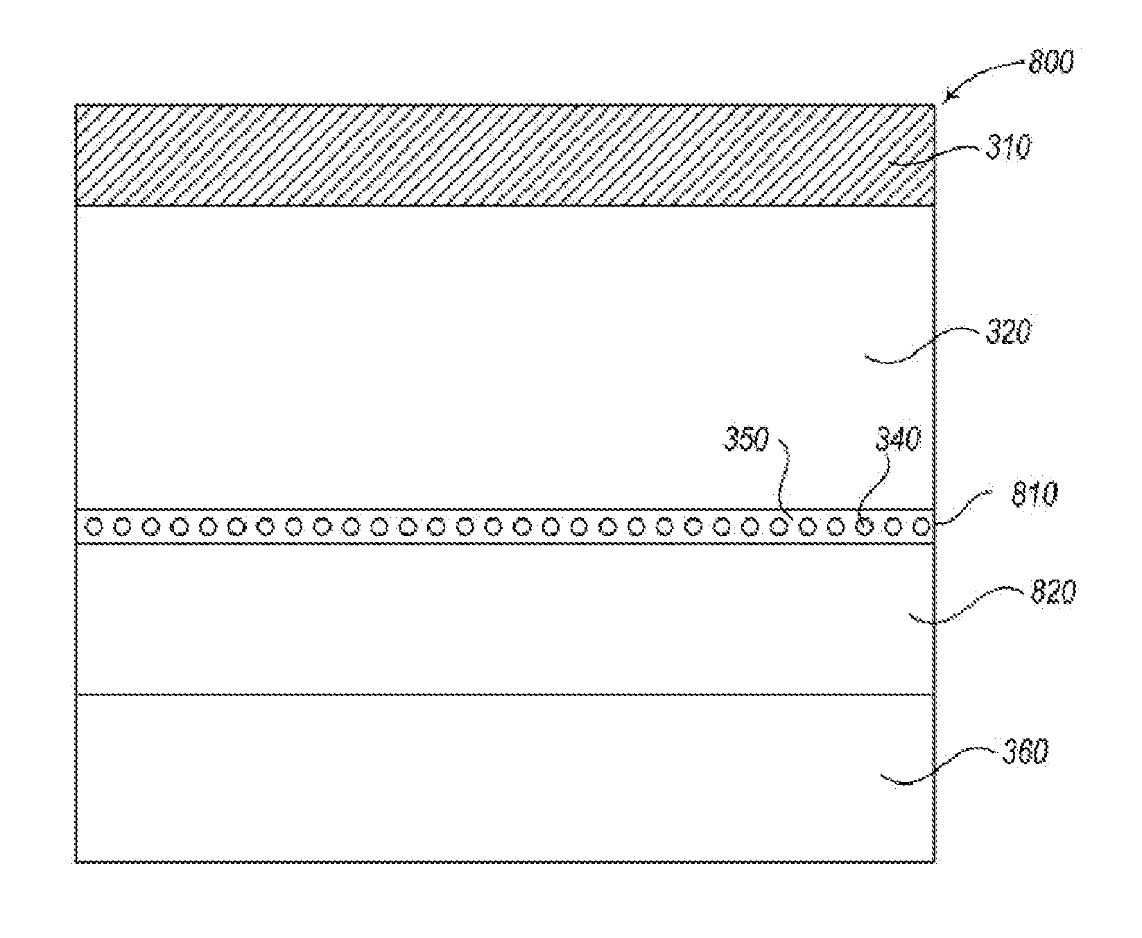
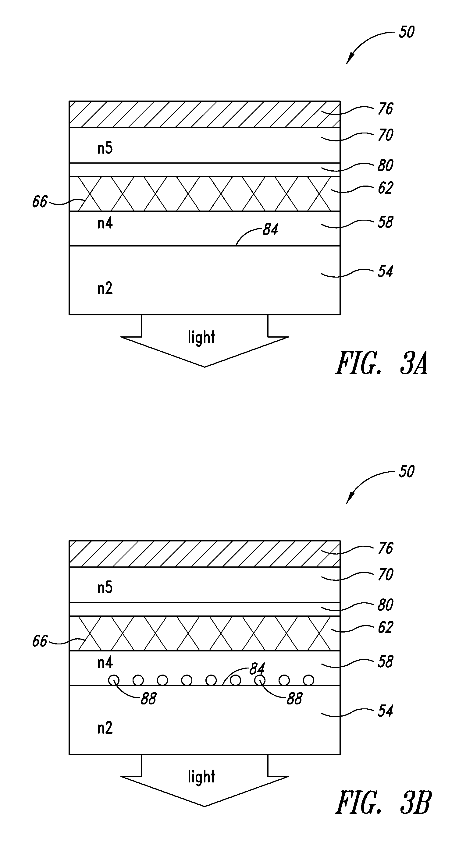
This patent describes opto-electrical devices with improved light out-coupling for outputting light or absorbing light. The patent describes an optical stack that includes a first electrode, an organic stack, and a nanostructure layer. The nanostructure layer includes a plurality of metal nanostructures that form a second electrode. The patent also describes a process for fabricating OLEDs using a solid-state transfer method. The technical effects of the patent include improved light out-coupling, reduced light loss, and improved photovoltaic cell efficiency.

Problems solved by technology

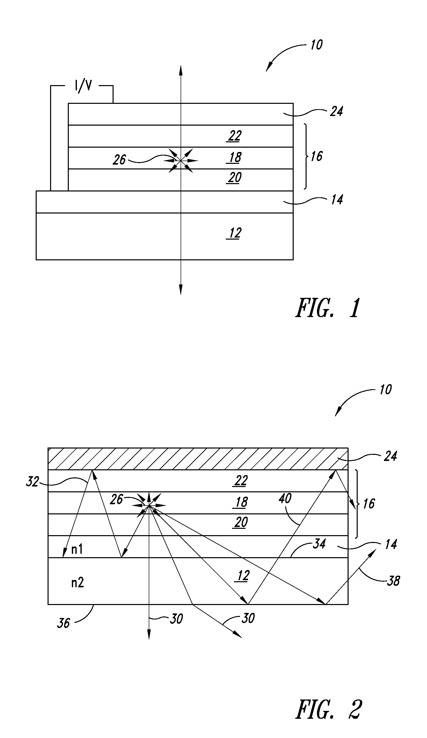
However, not all the light generated from the organic stack is capable of existing via the external mode.

Method used


Image

  • Opto-electrical devices incorporating metal nanowires
  • Opto-electrical devices incorporating metal nanowires
  • Opto-electrical devices incorporating metal nanowires

Examples


example 1

Synthesis of Silver Nanowires

[0154]Silver nanowires were synthesized by the reduction of silver nitrate dissolved in ethylene glycol in the presence of poly(vinyl pyrrolidone) (PVP) following the “polyol” method described in, e.g., Y. Sun, B. Gates, B. Mayers, & Y. Xia, “Crystalline silver nanowires by soft solution processing,” Nanoletters 2(2): 165-168, 2002. A modified polyol method, described in co-pending and co-owned U.S. patent application Ser. No. 11 / 766,552, produces more uniform silver nanowires at higher yields than does the conventional “polyol” method. This application is incorporated by reference herein in its entirety. Resulting nanowires primarily had lengths from about 13 μm to about 17 μm and diameters from about 34 nm to about 44 nm.

example 2

Standard Preparation of Coating Composition of Conductive Nanostructures

[0155]A typical coating composition for depositing metal nanowires comprises, by weight, from 0.0025% to 0.1% surfactant (e.g., a preferred range is from 0.0025% to 0.05% for ZONYL® FSO-100), from 0.02% to 4% viscosity modifier (e.g., a preferred range is 0.02% to 0.5% for hydroxypropyl methylcellulose (HPMC), from 94.5% to 99.0% solvent and from 0.05% to 1.4% metal nanowires.

[0156]The coating composition can be prepared based on a desired concentration of the nanowires, which is an index of the loading density of the final conductive film formed on the substrate.

[0157]The coating composition can be deposited on a substrate according to, for example, the methods described in co-pending U.S. patent application Ser. No. 11 / 504,822.

[0158]As understood by one skilled in the art, other deposition techniques can be employed, e.g., sedimentation flow metered by a narrow channel, die flow, flow on an incline, slit coati...

example 3

[0160]A polyimide coating solution (e.g., SUNEVER Polyimide (type 0821)) was first deposited on a substrate, spun on at 1500 rpm, followed by drying at 90° C., and curing for 30 min at 200° C. The haze and transmission of the resulting sample were 0.1% and 92.1%, respectively. The film thickness was measured at 1.2 microns.


PUM


Abstract

The present disclosure relates to OLED and PV devices including transparent electrodes that are formed of conductive nanostructures and methods of improving light out-coupling in OLED and input-coupling in PV devices.

Description

BACKGROUND[0001]1. Technical Field[0002]This disclosure generally relates to opto-electrical devices such as organic light-emitting diodes (OLEDs) and photovoltaic (PV) cells.[0003]2. Description of the Related Art[0004]An OLED emits light in response to an electric current. The light generation mechanism is based on radiative recombination of excitons of electrically excited organic compound(s). FIG. 1 shows a conventional OLED (10) formed on a substrate (12). An anode (14) is disposed on the substrate. The light-emitting layer takes the form of an organic stack (16) that includes a thin film of electroluminescent chemical compounds (18) flanked by two charge injection layers (20 and 22, one for electron injection and one for hole injection). A cathode (24) is disposed on the organic stack (16).[0005]The cathode and anode provide the contacts for an external circuitry to supply an electrical current, which in turn generates light (26) in the organic stack (16). In general, in a bot...

Claims


Application Information

Patent Timeline
IPC IPC(8): H01L51/50H01L31/0232H01L33/58
CPCH01L31/0232H01L33/58H01L51/50H01B1/22H01L51/442H01L51/5234H01L51/5262H01L51/5275Y02E10/549H05B33/28H01L2251/5369H01L51/44H01L51/5268Y02P70/50H10K71/60H10K71/80H10K30/82H10K50/858H10K2102/331H10K30/50H10K30/35H10K50/814H10K50/854H10K50/86H10K50/828H10K50/115H10K71/611H10K30/80H10K50/00H10K50/81H10K50/85H10K71/00H10K71/621H01L31/022491H01L31/1884
Inventor PSCHENITZKA, FLORIAN
Owner CHAMP GREAT INTL
Learn More