Structure for hermetic encapsulation of a device and an electronic component

a technology of electronic components and structures, applied in the field of encapsulation structures, can solve the problems of device(s) not being able to operate properly, the pressure and nature of the atmosphere in the cavity cannot be controlled, and the device(s) cannot operate properly

Active Publication Date: 2013-05-02
COMMISSARIAT A LENERGIE ATOMIQUE ET AUX ENERGIES ALTERNATIVES
View PDF21 Cites 10 Cited by
  • Summary
  • Abstract
  • Description
  • Claims
  • Application Information

AI Technical Summary

Benefits of technology

[0016]Thus there is a need to provide a solution for hermetically encapsulating, in the same cavity, at least one device with at least one electronic component, and making it possible to prevent any degassing caused by one or more material(s) of the electronic component from disrupting the operation of the device.
[0021]Thus, the getter material layer covering the electronic component exposed in the cavity makes it possible to trap and / or block the gases capable of being degassed by the electronic component in the cavity, for example after a thermal activation of the getter material.
[0024]Given that the device and the electronic component are arranged in the same cavity, such an encapsulation structure can therefore be produced with better compactness, and therefore with a lower production cost. Moreover, given that the gases trapped in the electronic component are not released in the cavity owing to the getter material layer, the performance of the device is not degraded.
[0040]This dielectric layer makes it possible to ensure electrical insulation between the electronic component and the getter material layer.
[0044]In another particular embodiment, the device may be produced on, or over, the getter material layer. Such a configuration makes it possible to superimpose the device on the integrated circuit, without disrupting the operation of the device. Such a configuration also makes it possible to easily electrically connect the electronic component to the device in consideration of the proximity of these two elements.
[0049]The encapsulation structure may also comprise at least one getter material portion distinct from the getter material layer and arranged in the cavity. This getter material portion can thus contribute to the control of the atmosphere in the cavity, and in particular contribute to obtaining the vacuum level required for the operation of the device.

Problems solved by technology

Such integration nevertheless presents problems in the operation of the device(s).
This gas release therefore makes it impossible to control the pressure and nature of the atmosphere in the cavity, and the device cannot therefore operate properly in this case.
Given that these getter material portions are intended to reach a vacuum level required for the device to operate correctly (for example, a primary vacuum close to 10−3 mbar for devices comprising resonant structures, for example accelerometers or gyrometers, or of the non-cooled infrared sensor type such as microbolometers) and the activation of this getter can be performed only once the cavity has been closed by heating the entire cavity as well as the elements present in the cavity, the gases released therefore significantly limit the vacuum level capable of being reached in the cavity, or may even result in gas saturation of the getter material.

Method used


Image

  • Structure for hermetic encapsulation of a device and an electronic component
  • Structure for hermetic encapsulation of a device and an electronic component
  • Structure for hermetic encapsulation of a device and an electronic component

Examples


first embodiment

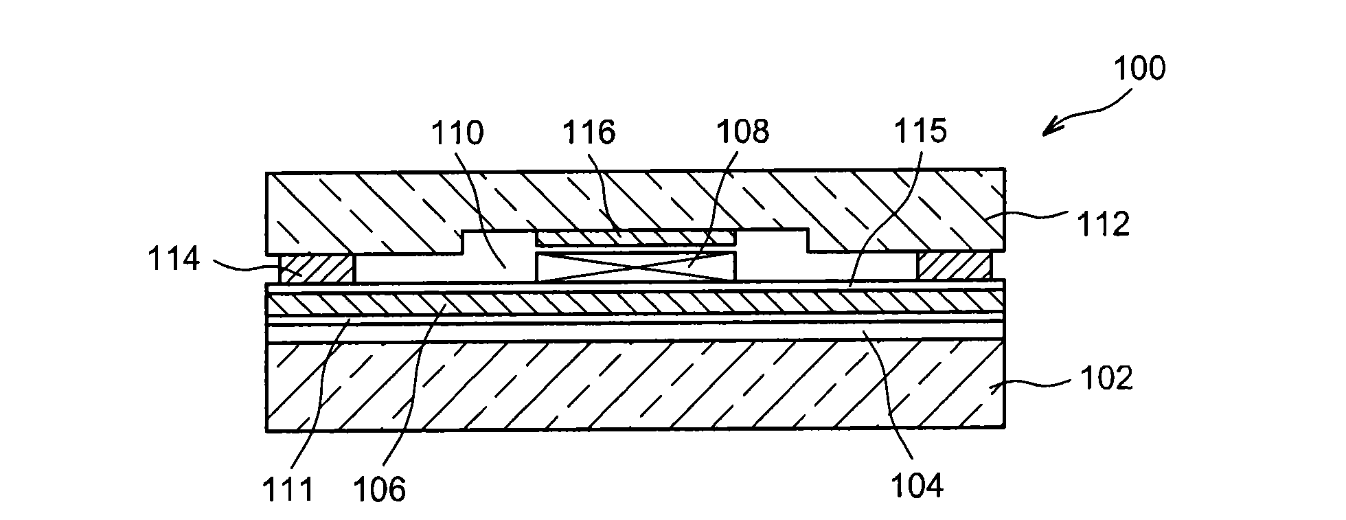
[0074]Reference is made to FIG. 1, which shows an encapsulation structure 100 according to a

[0075]The structure 100 comprises a first substrate 102 on which an integrated circuit 104 is produced, shown diagrammatically in FIG. 1 in the form of an active layer arranged on the first substrate 102. The integrated circuit 104 comprises in particular MOS-type devices such as CMOS transistors. The integrated circuit 104 is covered with a dielectric layer 111 covering in particular electrical contact pads of the integrated circuit 104 and enabling the integrated circuit 104 to be electrically insulating from the elements of the structure 100 intended to be produced on the integrated circuit 104.

[0076]The integrated circuit 104 and the dielectric layer 111 are covered with a getter material layer 106, comprising at least one getter material capable of performing gas absorption and / or adsorption, advantageously titanium, or zirconium, or an alloy comprising titanium and zirconium. The getter...

second embodiment

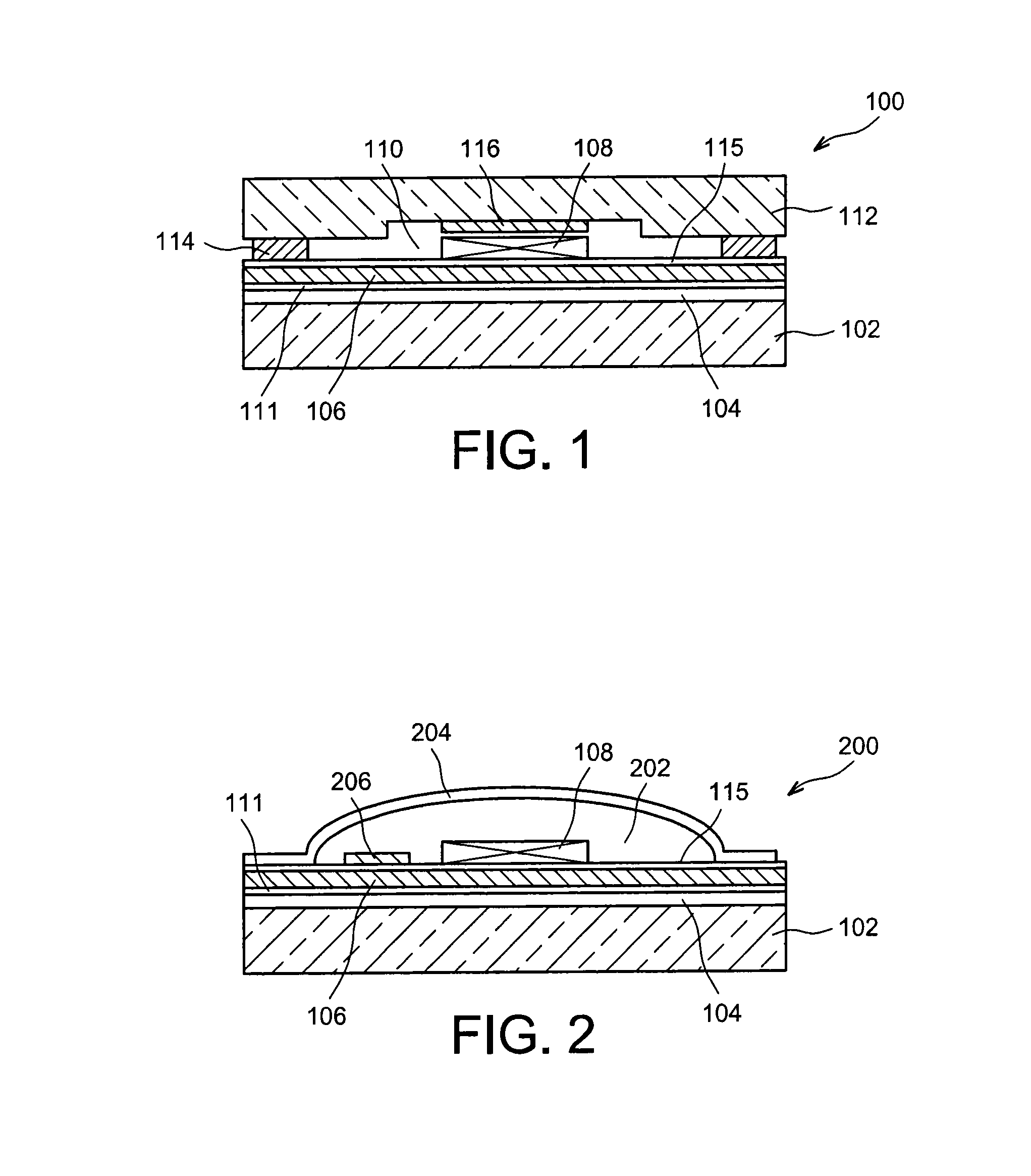
[0088]FIG. 2 shows an encapsulation structure 200 according to a

[0089]Like the encapsulation structure 100 described above, the encapsulation structure 200 comprises the first substrate 102, the integrated circuit 104 covered with the dielectric layer 111, the getter material layer 106 covering the dielectric layer 111, as well as the device 108. As above, a dielectric layer 115 may cover the getter material layer 106 so as to electrically insulate the device 108 from the getter material layer 106.

[0090]Unlike the encapsulation structure 100 comprising a cap formed by the second substrate 112 secured to the first substrate 102, the encapsulation structure 200 comprises a cavity 202 in which the device 108 and the integrated circuit 104 are encapsulated, and formed between the first substrate 102 and one or more thin films 204 produced by a TFP-type process (including in particular the production of a sacrificial material portion enabling the deposition of the layers intended to form...

third embodiment

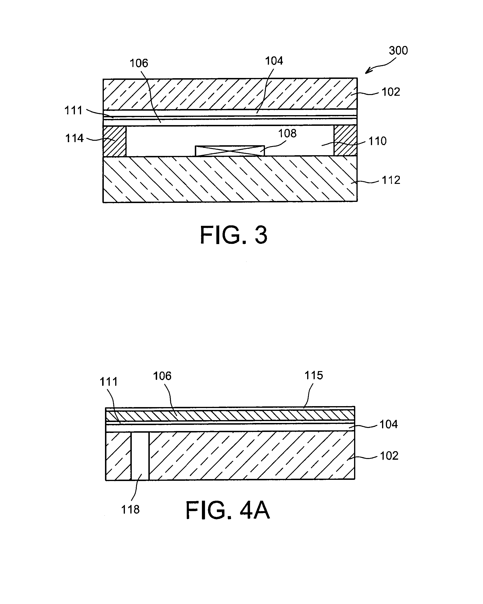
[0093]Reference is made to FIG. 3, which shows an encapsulation structure 300 according to a

[0094]Like the encapsulation structure 100, the encapsulation structure 300 comprises the cavity 110 formed between the first substrate 102 and the second substrate 112 and in which the device 108 and at least one part of the integrated circuit 104 are encapsulated. However, in this third embodiment, the integrated circuit 104 is produced on the first substrate 102, which forms the cap of the cavity 110. The device 108 is therefore produced not on the integrated circuit 104, but directly on and / or in the second substrate 112. As in the previous embodiments, the integrated circuit 104 is covered by the getter material layer 106 making it possible to absorb and / or adsorb the gases released by the materials of the integrated circuit 104 during the thermal activation of the getter material present in the encapsulation structure 300. While not shown, it is possible for one or more getter material ...


PUM

PropertyMeasurementUnit
thicknessaaaaaaaaaa
diameteraaaaaaaaaa
diameteraaaaaaaaaa

Abstract

An encapsulation structure comprising at least one hermetically sealed cavity in which at least the following are encapsulated:a device,an electronic component produced on a first substrate, anda getter material layer covering the electronic component in order to block the gases capable of being degassed by the electronic component,and in which the device is not covered by the getter material layer.

Description

TECHNICAL FIELD[0001]The invention relates to an encapsulation structure including a hermetic cavity in which a device is encapsulated, for example a microsystem or a micro-component in particular of the MEMS (microelectromechanical system), NEMS (nanoelectromechanical system), MOEMS (micro-opto-electro-mechanical system), NOEMS (nano-opto-electro-mechanical system) type or an infrared microsensor, or more generally any device intended to be encapsulated under a controlled atmosphere, with one or more electronic components, forming, for example, an integrated circuit, and a getter material.[0002]The invention also relates to a process for encapsulating at least one device enabling such an encapsulation structure to be produced.PRIOR ART[0003]Some devices such as those of the MEMS, NEMS, MOEMS, NOEMS type or infrared microsensors must, for successful operation, be hermetically enclosed or encapsulated in a cavity of which the atmosphere is controlled (control in particular of the nat...

Claims


Application Information

Patent Timeline
Patent Type & Authority Applications(United States)
IPC IPC(8): H01L23/26H01L21/54
CPCB81B2207/012B81C1/00285H01L2924/14H01L2924/13091H01L23/26H01L2924/0002
Inventor BAILLIN, XAVIERPORNIN, JEAN-LOUIS
Owner COMMISSARIAT A LENERGIE ATOMIQUE ET AUX ENERGIES ALTERNATIVES
Why Eureka
Try Eureka