Eureka AIR delivers breakthrough ideas for toughest innovation challenges, trusted by R&D personnel around the world.

Nonvolatile latch circuit, nonvolatile flip-flop circuit, and nonvolatile signal processing device

Active Publication Date: 2013-05-02
PANASONIC SEMICON SOLUTIONS CO LTD
View PDF5 Cites 8 Cited by
  • Summary
  • Abstract
  • Description
  • Claims
  • Application Information

AI Technical Summary

Benefits of technology

The present invention allows for the placement of nonvolatile latch circuits and flip-flop circuits in logic circuits, which can improve their operation speed. The nonvolatile circuits use a high voltage to record information on a memory element, but this is not necessary for the present invention. The initial resistance value of the memory element can be changed to desired state by applying a low voltage. This results in a reliable and stable memory element that can be used in logic circuits.

Problems solved by technology

However, once the power source to the latch circuits is turned off, the state of each latch circuit is not held but is lost (volatile).
Although power saving LSIs have been developed along with the progress of finer semiconductor process, steering of leakage current has become difficult because of the progress, and thus the power saving LSIs in use of only finer semiconductor process are approaching the limit.
However, when the power source for a block is turned off, the logic state of the block is lost, and thus the approach cannot be performed on a circuit block for which continuous processing is needed.
However, as an example of application to an LSI of a nonvolatile latch circuit in the conventional art, a floating gate memory element (hereinafter referred to as a flash memory) is utilized as a program recording memory of FPGA (Field-Programmable Gate Arrays) or FPLD (Field-Programmable Logic Devices), and thus the application is limited to a memory area formed as a separate area from a logic circuit.
This is because erasing or writing information of or to a flash memory needs a time of the order of μs, and thus the duty cycle of the flash memory cannot be synchronized with the duty cycle of the logic circuit.
In the case where such a memory is individually installed in each latch circuit in the logic circuit, even when an operation of each latch circuit is completed, recording of information (logic state of the latch circuit) to the memory is not completed, and thus high-speed operation performance of the logic circuit is impaired.
However, there is a problem in that in the case of a sudden power off, all the latch states in the logic circuit cannot be transferred to the flash memory in time, and thus the recording cannot be completed.
Therefore, a write operation to the flash memory cannot be directly performed based on an output signal of the logic circuit.
Furthermore, the manufacturing process of flash memory is complicated in general, and thus forming the logic circuit and the flash memory on the same substrate makes the process even more complicated.
In addition, after the transistors that constitute the logic circuit are formed, high-heat process or the like is involved, and therefore the performance of the transistors may be impaired.

Method used


Image

  • Nonvolatile latch circuit, nonvolatile flip-flop circuit, and nonvolatile signal processing device
  • Nonvolatile latch circuit, nonvolatile flip-flop circuit, and nonvolatile signal processing device
  • Nonvolatile latch circuit, nonvolatile flip-flop circuit, and nonvolatile signal processing device

Examples


embodiment 1

Configuration of Variable Resistance Element

[0108]First, a variable resistance element used for a nonvolatile latch circuit and a flip-flop circuit of the present invention is described.

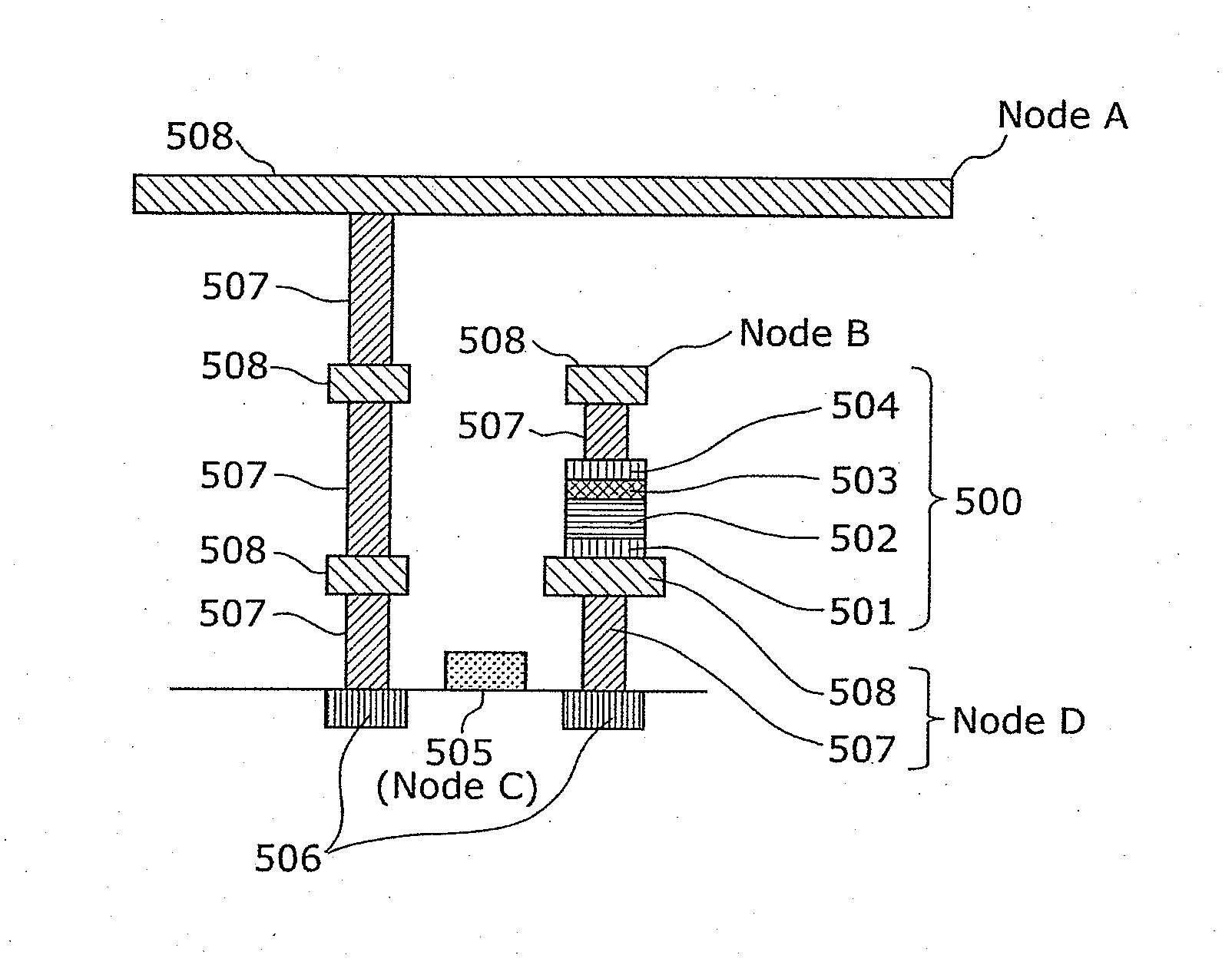
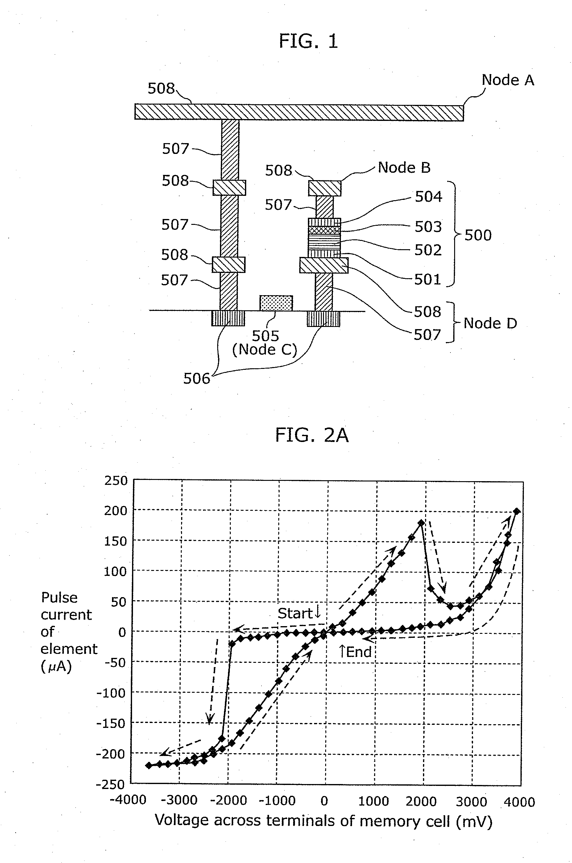
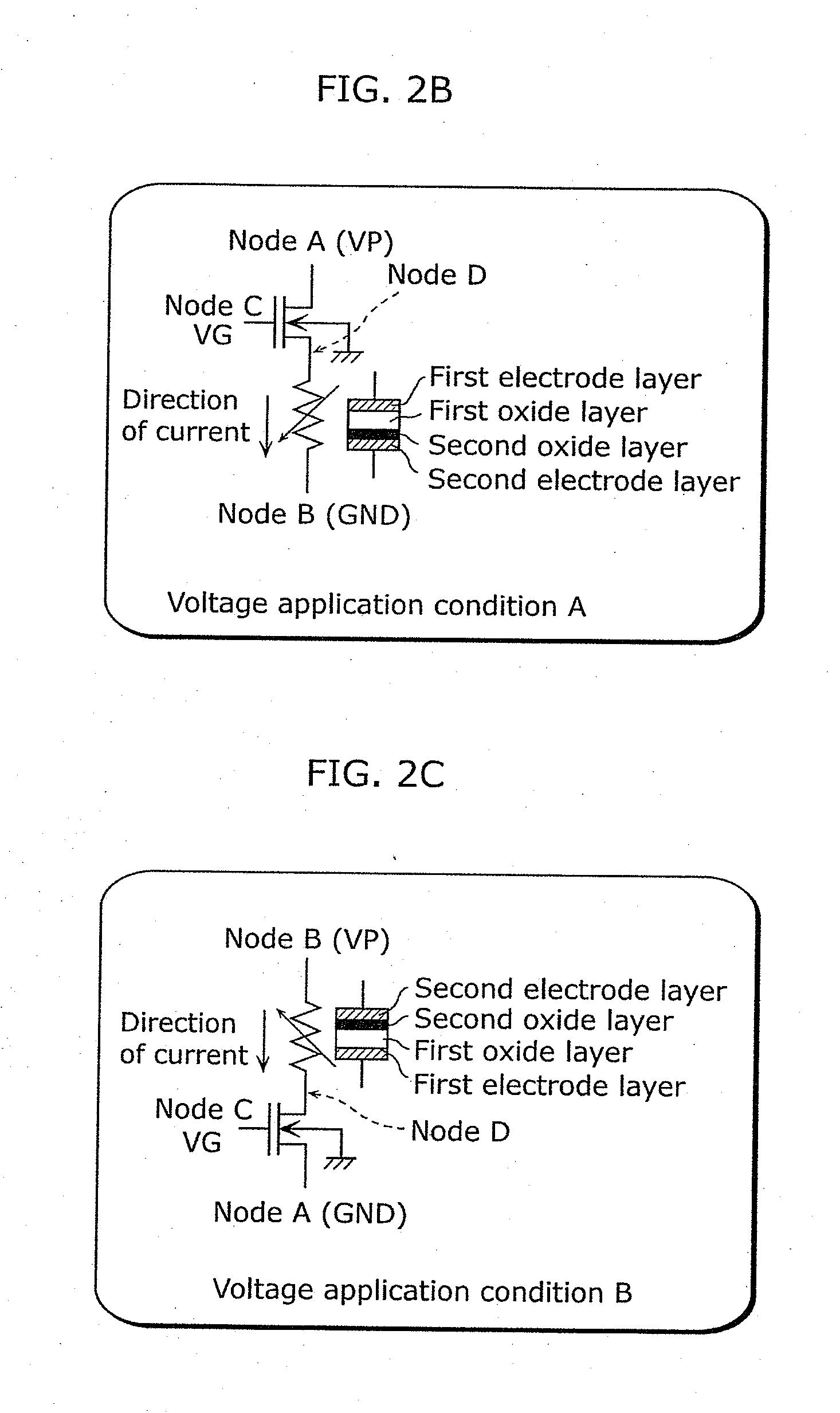
[0109]FIG. 1 is an element configuration diagram illustrating an example of the schematic configuration of a variable resistance element having a nonvolatile latch circuit according to Embodiment 1 of the present invention. A variable resistance element 500 illustrated in FIG. 1 is formed on a semiconductor process structure including an ordinary CMOS transistor, and is connected to a semiconductor substrate using, for example, a plug layer 507 on the semiconductor substrate. An MOS transistor including a source-drain region 506 and a gate oxide layer 505 is formed on the substrate.

[0110]The variable resistance element 500 includes a first electrode layer 501 which is a first electrode formed on a metal wiring layer 508, a second electrode layer 504 which is a second electrode, and a first variable r...

embodiment 2

[0185]Next, Embodiment 2 of the present invention will be described with reference to FIGS. 12 to 14.

[0186]FIG. 12 is a circuit configuration diagram of a nonvolatile latch circuit according to Embodiment 2 of the present invention. In FIG. 12, FIGS. 13A and 13B, the components labeled with the same symbols as those in FIG. 3 indicate the same components. However, the gate widths of the transistors 6 and 7 are assumed to be the same as described below. The nonvolatile latch circuit 200 according to the present embodiment differs from the nonvolatile latch circuit 100 illustrated in FIG. 3 in that the control signal inputted to the gate of the transistor 6 via Ctrl1 terminal, and the control signal inputted to the transistor 7 via Ctrl2 terminal are separately inputted. Because of this modification, the store operation and the forming operation in Embodiment 2 are different from those in Embodiment 1.

[0187]As described in Embodiment 1, it is preferable to limit the current flow for a...

embodiment 3

[0205]Next, Embodiment 3 of the present invention will be described with reference to FIGS. 16A and 16B.

[0206]FIG. 16A is a circuit configuration diagram of a nonvolatile flip-flop circuit according to Embodiment 3 of the present invention. FIG. 16B is a diagram illustrating a logic table of the nonvolatile flip-flop circuit according to Embodiment 3 of the present invention. In FIG. 16A, the components labeled with the same symbols as those in FIG. 4 indicate the same components. A nonvolatile flip-flop circuit 300 according to the present embodiment differs from the nonvolatile latch circuit 100 of FIG. 4 in that the inverter circuits 20 and 21 are replaced by NAND gate circuits 50 and 51 with 2 inputs.

[0207]As described in Embodiment 1, when an input to Ctrl1 terminal and Ctrl2 terminal is GND level, and the transmission gates TMG2 and TMG3 are set to off state, the transistors 6 and 7, the variable resistance element 1, the summing amplifier circuit 22, and the inverter circuit ...


PUM


Abstract

A nonvolatile latch circuit according to the present invention wherein the outputs of an inverter circuit and other inverter circuit which are cross-coupled are connected to each other via a series circuit in which a transistor, a variable resistance element, and other transistor are connected in this order; a store operation and a restore operation for a latch state are controlled by application of a voltage to control terminals of the transistor and the other transistor; and both end potentials of the variable resistance element are summed, an amount of the sum is amplified and inverted, and the inverted amount is returned to an input of the inverter circuit or the other inverter circuit, thereby restoring a logic state in which a forming process of the variable resistance element can be performed.

Description

TECHNICAL FIELD[0001]The present invention relates to a nonvolatile latch circuit, a nonvolatile flip-flop circuit, and a nonvolatile signal processing device. Particularly, the present invention relates to a nonvolatile digital signal processing device which can restore a state of signal processing before a power supply is turned off, by a nonvolatile latch circuit restoring the state of the nonvolatile latch circuit which holds the state even when the power supply is turned off.BACKGROUND ART[0002]A great number of microcomputers and logic LSIs which include a digital circuit are used in electronic products.[0003]In a digital circuit such as a microcomputer or an LSI, a latch circuit which temporarily holds digital signals for intermediate processed content, or a register circuit (hereinafter, collectively referred to as simply latch circuit) such as a flip-flop which stores one bit of digital information is used on a signal processing path. The latch circuit holds two states, hig...

Claims


Application Information

Patent Timeline
IPC IPC(8): G11C13/00
CPCG11C11/4125H03K3/0375H03K3/356008H01L27/2436H01L45/08H01L45/1233H01L45/146G11C13/0021H10B63/30H10N70/24H10N70/8833H10N70/826
Inventor KATOH, YOSHIKAZU
Owner PANASONIC SEMICON SOLUTIONS CO LTD
Why Eureka
Eureka Blog
Learn More