Charged particle optical system and scribing apparatus
a technology of optical system and charge particle, applied in the direction of beam deviation/focusing by electric/magnetic means, instruments, therapy, etc., can solve the problem of uniform deformation of the member, achieve the effect of enhancing space efficiency, shortening arrangement distance, and reducing distribution of gaps
- Summary
- Abstract
- Description
- Claims
- Application Information
AI Technical Summary
Benefits of technology
Problems solved by technology
Method used
Image
Examples
example 1
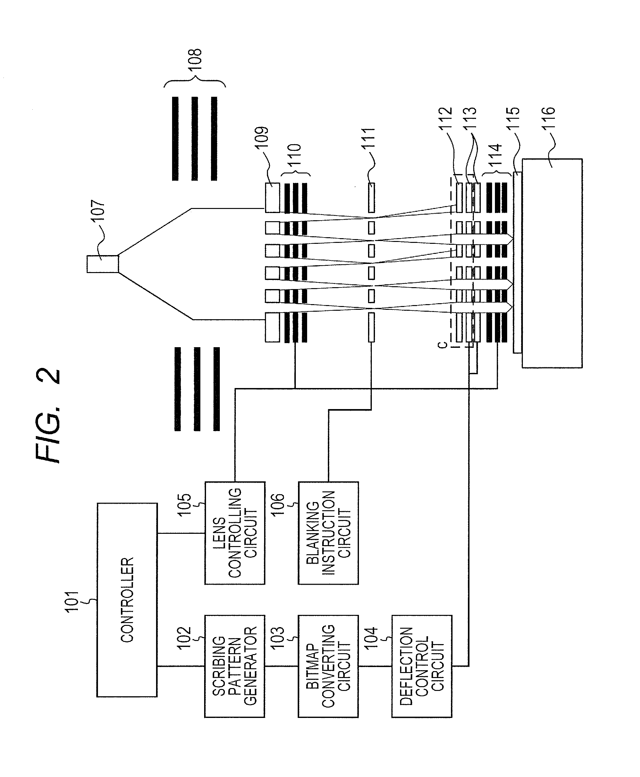
[0032]FIG. 2 illustrates a configuration of a charged particle scribing apparatus using a charged particle optical system of the present invention. Here, the charged particle is an electron. Electron beams are emitted from an electron source 107, are converted into parallel beams by a collimating lens 108, and are irradiated on an aperture array 109. A plurality of the electron beams which have been divided by the aperture array 109 are individually focused by a focusing lens array 110 that is controlled by a lens controlling circuit 105, and form images on a blanker array 111. The blanker array 111 is a device having individually deflecting electrodes therein. The blanker array turns the individual beams ON / OFF according to a scribing pattern based on a blanking signal generated by a scribing pattern generator 102, a bit map converting circuit 103, and a blanking instruction circuit 106. When the beam is in the ON state, a voltage is not applied to the deflecting electrodes of the ...
example 2
[0043]Example 2 of the present invention will be described below with reference to FIGS. 6A and 6B. The portions having the same functions and effects as in Example 1 are denoted by the same symbols, and the description will be omitted. The present example is different from Example 1 in a point that two electrostatic deflectors 113 are used so as to form two-stage deflectors. FIG. 6A illustrates a configurational cross section of a unit of the present example which almost corresponds to a unit shown by a dashed line c of FIGS. 2A and 2B. The two electrostatic deflectors 113a and 113b are assembled under a stop aperture array 112 as is illustrated in the figure.
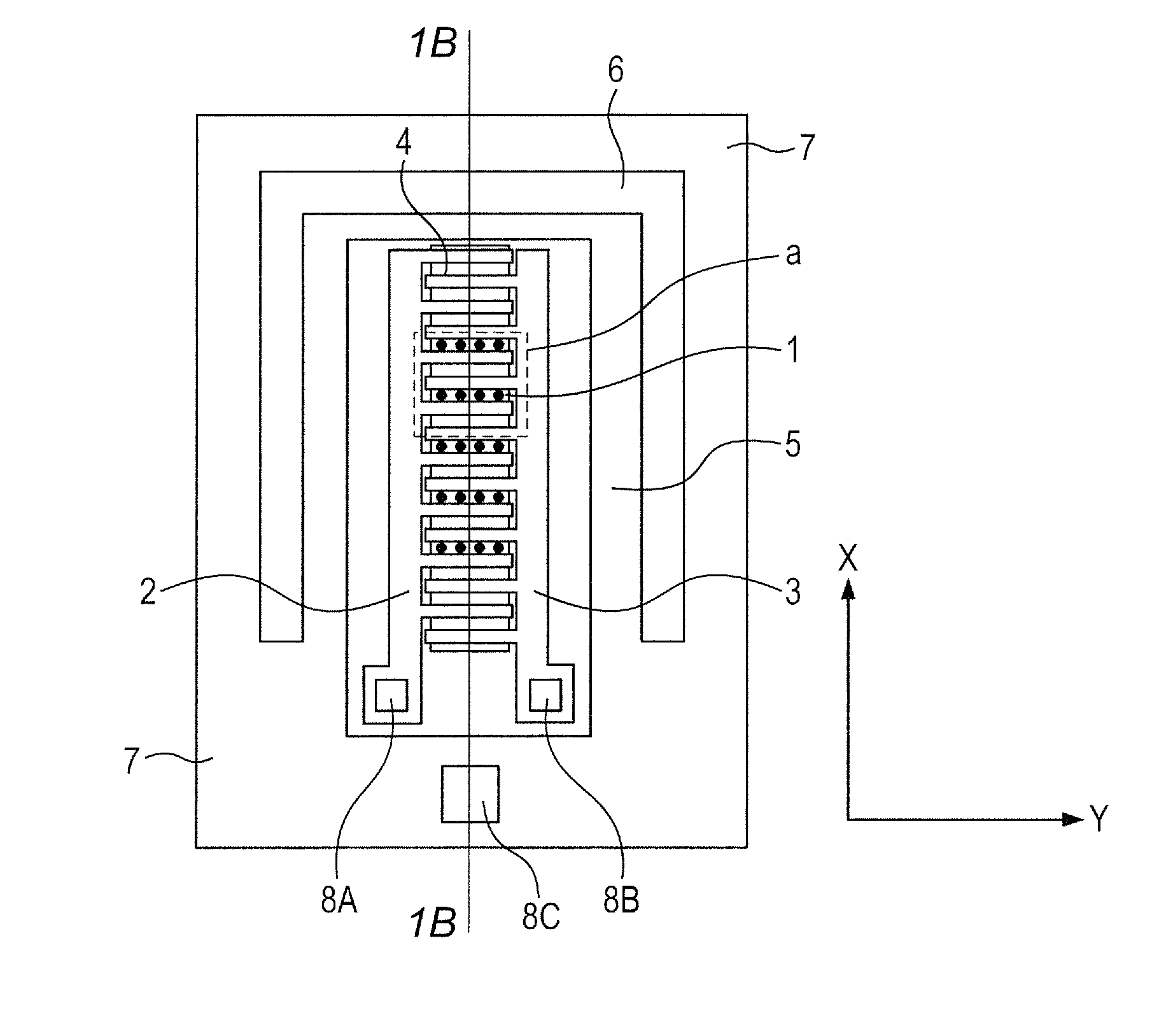
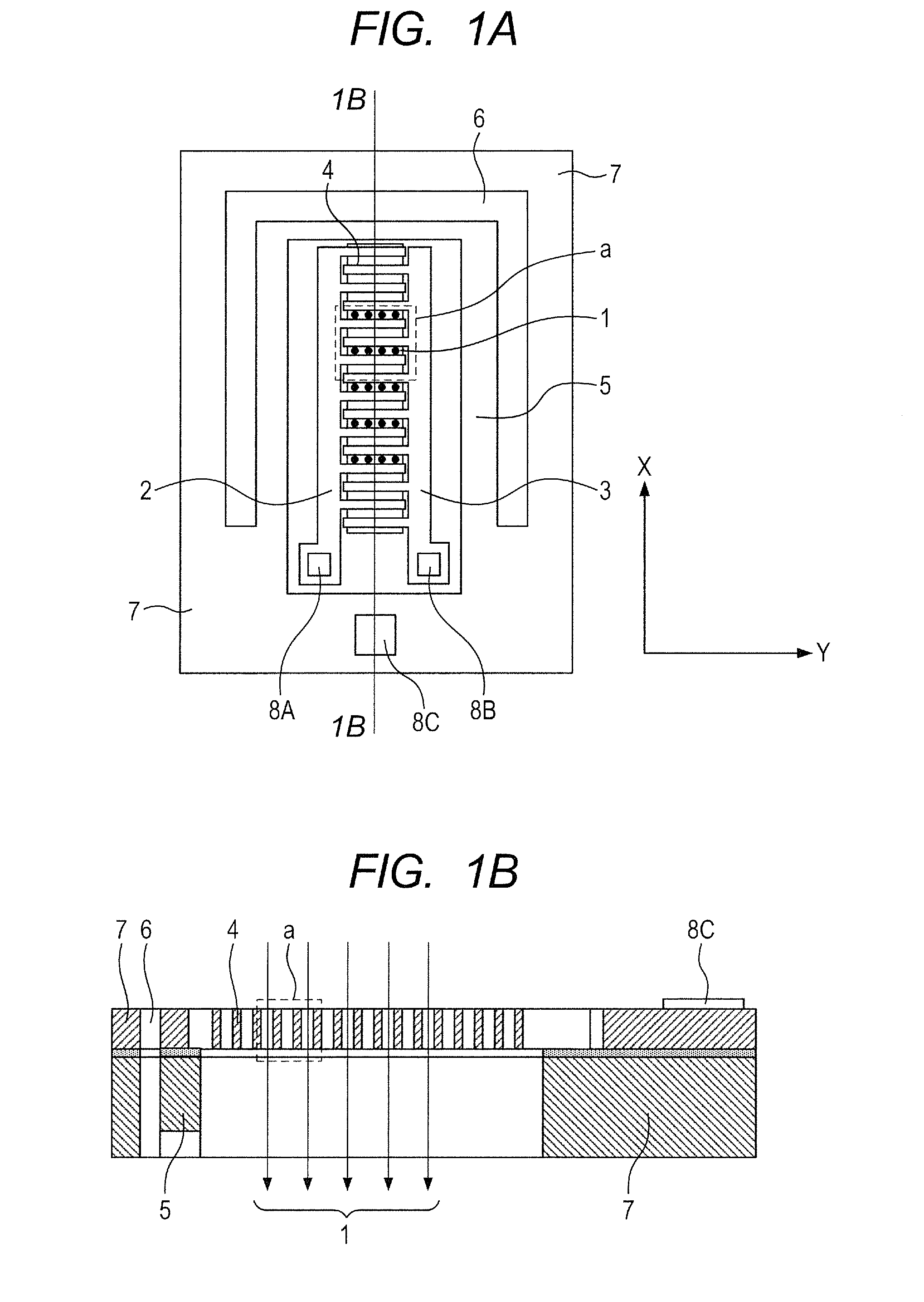
[0044]In the present example, the electrostatic deflectors 113a and 113b have a cantilever beam structure pivotal in relation to a fixing portion 7 by a stress suppressing structure 6 (slit), as is illustrated in FIGS. 1A and 1B. The cantilever beam structure of the two electrostatic deflectors is assembled so that fixed ends ...
example 3
[0052]Example 3 of the present invention will be described below with reference to FIG. 7A. The portions having the same functions and effects as in Example 1 are denoted by the same symbols, and the description will be omitted. The present example is different from Example 1 in a stress suppressing structure which an electrostatic deflector 113 has. FIG. 7A illustrates a top plan view of an electrostatic deflector 113. A spring 6 having a spring constant in the direction shown by the arrow k is arranged as the stress suppressing structure. Even though deformation Ax is transmitted to a fixing portion 7, an electrode supporting portion 5 receives only a deforming force of kAx due to the spring constant k. The deforming force transmitted to the electrode supporting portion 5 can be reduced by appropriately selecting the spring constant k.
[0053]In addition, the spring 6 illustrated in the figure has such a structure that the spring 6 is ductile in the arrow k direction but is firm in ...
PUM
 Abstract
Description
Claims
Application Information


