Electrical overstress protection using through-silicon-via (TSV)

a technology of throughsilicon and overstress protection, which is applied in the direction of semiconductor/solid-state device details, diodes, radiation controlled devices, etc., can solve the problems of pn junctions that cannot be blocked in the reverse direction, pn junctions that could eventually reach avalanche breakdown, and catastrophic failure of pn junctions

Active Publication Date: 2013-05-16
ANALOG DEVICES INC
View PDF0 Cites 21 Cited by
  • Summary
  • Abstract
  • Description
  • Claims
  • Application Information

AI Technical Summary

Problems solved by technology

However, when a high enough voltage is applied in the reverse direction, the PN junction could eventually reach avalanche breakdown, at which point it is no longer able to block currents in the reverse direction and a relative small current may conduct in the reverse direction.
This relative small current in the reverse direction may cause catastrophic failure within the PN junction.
However, if a reverse bias as high as the avalanche breakdown is applied, the photodiode may be permanently damaged and could operate erroneously.
The electrostatic discharge (ESD) effects commonly known to occur in electrical circuits may cause sudden and unexpected high voltage charges over semiconductor devices in both forward and reverse directions.
However, this approach may not be appropriate for semiconductor devices such as photodiodes situated in a photodiode array.

Method used


Image

  • Electrical overstress protection using through-silicon-via (TSV)
  • Electrical overstress protection using through-silicon-via (TSV)
  • Electrical overstress protection using through-silicon-via (TSV)

Examples


Embodiment Construction

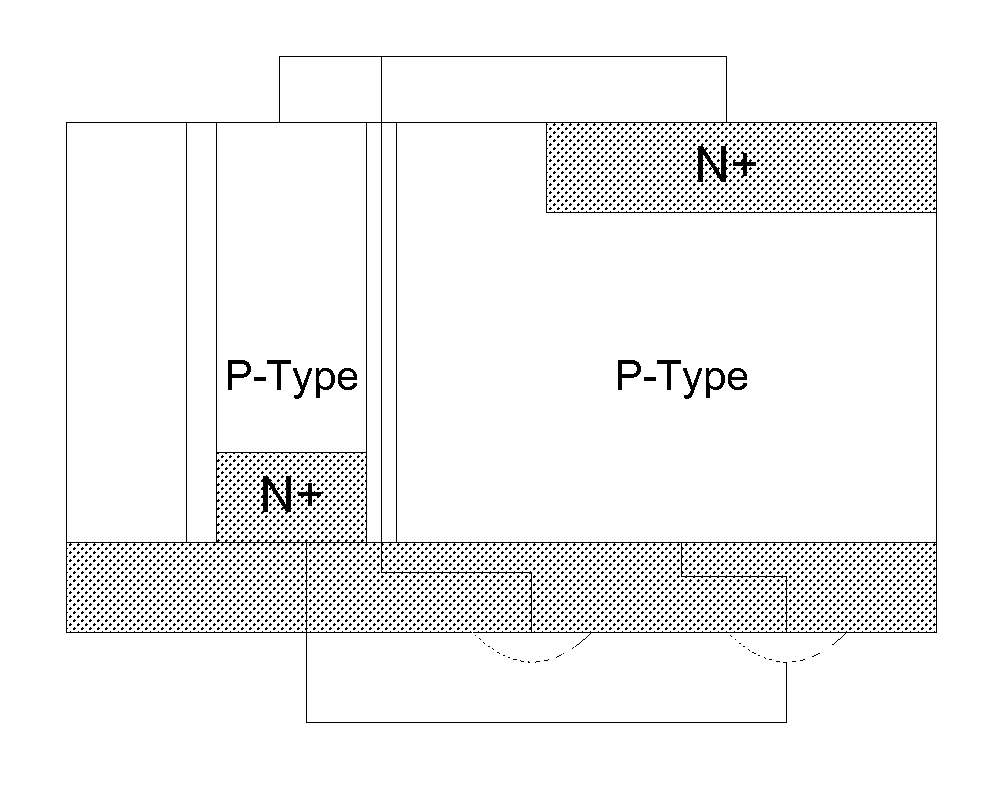
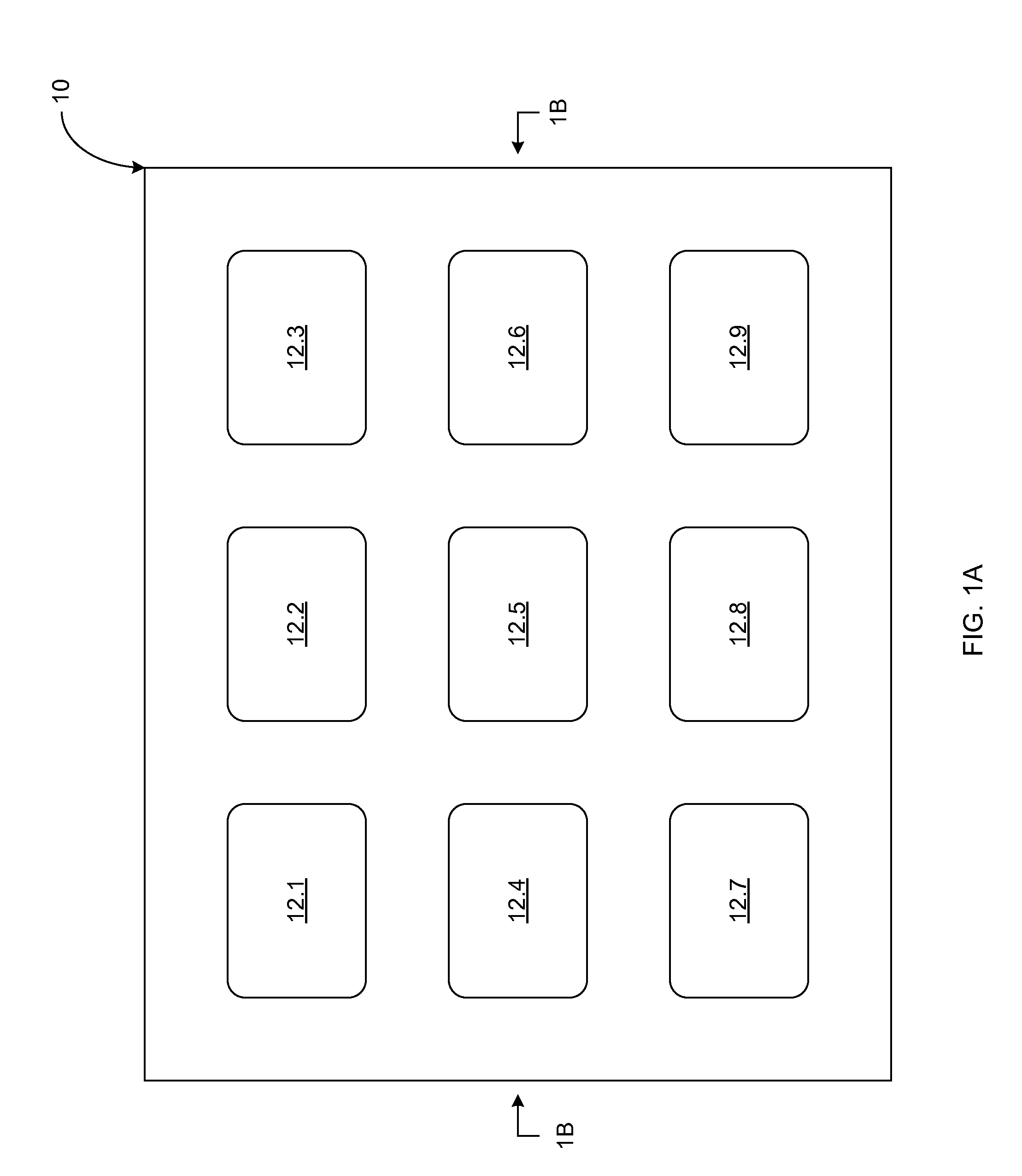
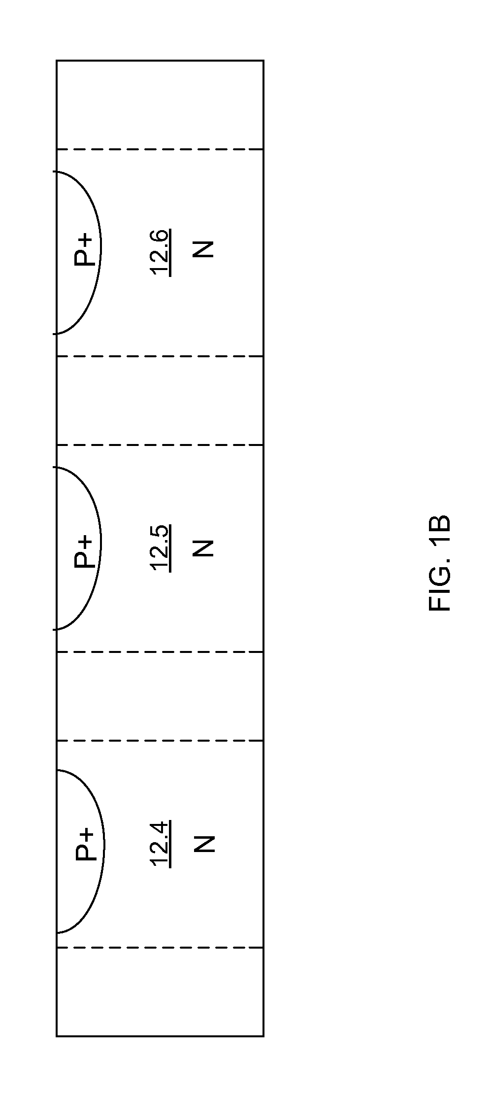
[0012]FIG. 1A illustrates a top view of a photodiode panel 10 that includes a plurality of photodiodes 12.1 to 12.9. FIG. 1B illustrates a cross-sectional view of the photodiode panel 10 as shown in FIG. 1A. Referring to FIGS. 1A and 1B, the photodiode panel 10 may include an N-doped semiconductor substrate on a single die, on which selected regions are implanted with P dopants, so that PN junctions for photodiodes 12.1 to 12.9 may be formed in those regions. The N-doped silicon may be connected to cathodes (not shown), and the P-type silicon may be connected to anodes (not shown). During ESD events, electrical discharges may suddenly appear either in the forward direction (anode-cathode) or in the reverse direction (cathode-anode). The photodiodes in the photodiode panel 10 may accommodate forward voltage stress (anode-cathode). However, the reverse voltage stress (cathode-anode), even at relative low stress level, may cause the photodiode panel to fail catastrophically. Because of...


PUM


Abstract

A semiconductor device formed on a substrate includes a first diode junction formation, a second diode junction formation, and at least one through-silicon-via (TSV), in which a cathode and an anode of the first diode are cross-connected to an anode and cathode of the second diode through the at least one TSV for achieving electrical robustness in through-silicon-via based integrated circuits, including photosensitive devices and circuits for signal processing applications.

Description

FIELD OF THE INVENTION[0001]The present invention is generally directed to a semiconductor device that includes structures to protect the device from electrical overstress conditions. In particular, the present invention utilizes through-silicon-via (TSV) technology to create electrical overstress protections on the same semiconductor substrate for the semiconductor device.BACKGROUND INFORMATION[0002]Semiconductor devices, including PN junctions, typically conduct current in the forward direction and block current in the reverse direction. When operating in the forward direction, the PN junction is capable of conducting high current density (measured in terms of amperes per unit area), while maintaining relatively low power dissipation. However, when a high enough voltage is applied in the reverse direction, the PN junction could eventually reach avalanche breakdown, at which point it is no longer able to block currents in the reverse direction and a relative small current may condu...

Claims


Application Information

Patent Timeline
Patent Type & Authority Applications(United States)
IPC IPC(8): H01L27/144H01L27/06
CPCH01L27/0255H01L29/0646H01L27/1446H01L23/481H01L2924/0002H01L2924/00
Inventor HU, LEJUNPARTHASARATHY, SRIVATSANCOLN, MICHAELSALCEDO, JAVIER
Owner ANALOG DEVICES INC
Why Eureka
Try Eureka