Transparent conductive film, substrate with transparent conductive film, and organic electroluminescence element using the same

a technology of transparent conductive film and organic electroluminescence element, which is applied in the direction of non-metal conductors, instruments, conductors, etc., can solve the problems of increased cost in the manufacturing of devices using organic el elements, poor smoothness, and easy breakage of materials with respect to bending or physical stress, so as to achieve uniform electrical conductivity, suppress mixing of one layer with the other, and smooth surface

Active Publication Date: 2013-05-16
PANASONIC INTELLECTUAL PROPERTY MANAGEMENT CO LTD
View PDF2 Cites 14 Cited by
  • Summary
  • Abstract
  • Description
  • Claims
  • Application Information

AI Technical Summary

Benefits of technology

[0014]According to the transparent conductive film according to the present invention, since the third transparent resin layer including the resin which is insoluble in water or has water resistance is provided between the first transparent resin layer and the second transparent resin layer, when the first transparent resin layer and the second transparent resin layer are formed, mixing of one of these layers with the other layer can be suppressed. In addition, since the first transparent resin layer and the second transparent resin layer are not mixed, one of these layers can be less likely to be damaged by the other. Therefore, a transparent conductive film is obtained which has a smooth surface and uniform electrical conductivity.

Problems solved by technology

However, an electrode for which ITO is used as the material is fragile and is easy to break with respect to bending or physical stress.
In addition, in order to improve the electrical conductivity of the electrode for which ITO is used, a high deposition temperature and / or a high anneal temperature are needed, and thus there is a concern over increased costs in the manufacturing of a device using an organic EL element.
Thus, the surface is rugged and has poor smoothness.
When the material of each transparent resin layer is mixed or one of the layers is damaged as described above, there is the possibility that electrical conductivity is decreased or made ununiform.

Method used


Image

  • Transparent conductive film, substrate with transparent conductive film, and organic electroluminescence element using the same
  • Transparent conductive film, substrate with transparent conductive film, and organic electroluminescence element using the same
  • Transparent conductive film, substrate with transparent conductive film, and organic electroluminescence element using the same

Examples


example 1

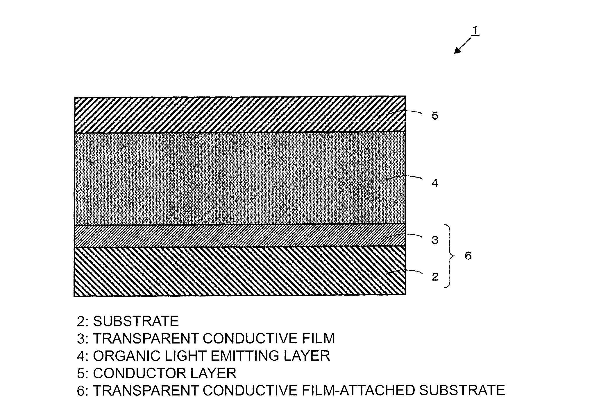
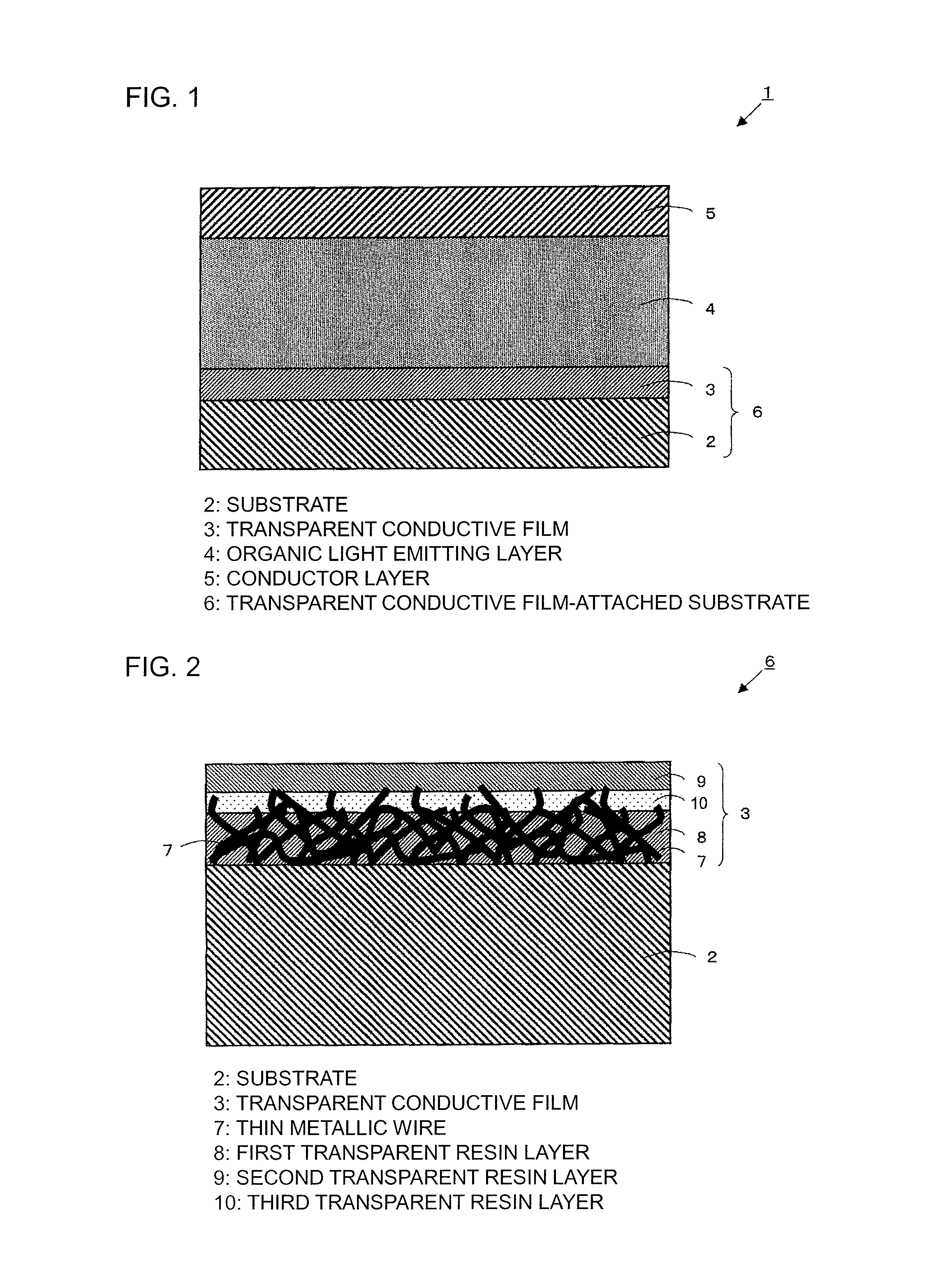
[0068]As a substrate, alkali-free glass No. 1737 manufactured by Corning Incorporated (the refractive index of light having a wavelength of 500 nm is 1.50 to 1.53) was prepared. Next, the previously-produced material of the first transparent resin layer which material includes the thin metallic wires was applied onto the substrate by a spin coating method such that the thickness was 100 nm, and was heated for 5 minutes at 100° C. By so doing, the first transparent resin layer was formed on the substrate. Next, the material of the first porous layer was applied onto the first transparent resin layer such that the thickness was 30 nm, and was heated for 5 minutes at 100° C. By so doing, a porous layer having a contact angle of 30 degrees with respect to water was formed on the first transparent resin layer. Next, the material of the second transparent resin layer was applied onto the porous layer such that the thickness was 100 nm, and was heated for 5 minutes at 100° C. By so doing, ...

example 2

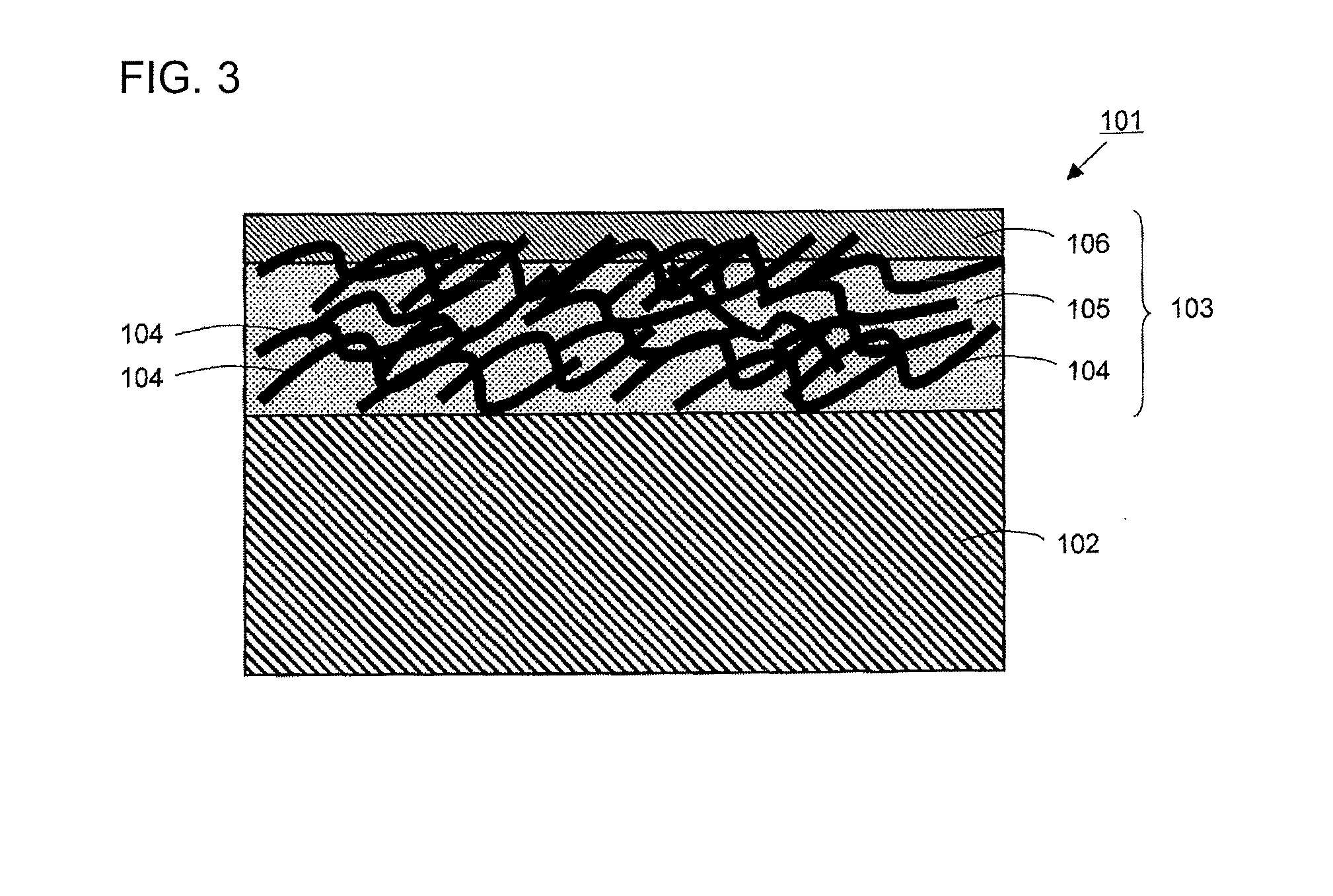
[0069]The sample of Example 2 was produced in the same manner as Example 1 described above, except that instead of the material of the first porous layer, the material of the second porous layer was used to form a second porous layer having a pore diameter of 10 nm and a contact angle of 60 degrees with respect to water.

example 3

[0070]The sample of Example 3 was produced in the same manner as Example 1 described above, except that the material of the first porous layer was applied onto the substrate such that the thickness was 300 nm.


PUM

PropertyMeasurementUnit
pore diameteraaaaaaaaaa
thicknessaaaaaaaaaa

Abstract

A transparent conductive film includes a first transparent resin layer including a plurality of thin metallic wires, a second transparent resin layer containing a conductive polymer, and a third transparent resin layer provided between the first transparent resin layer and the second transparent resin layer. The second transparent resin layer contains a resin which is soluble in water, and the third transparent resin layer contains a resin which is insoluble in water or has water resistance. The third transparent resin layer can suppress mixing of the second transparent resin layer with the first transparent resin layer and can make the second transparent resin layer less likely to be damaged by the first transparent resin layer. Therefore, a surface of the second transparent resin layer is made smooth and electrical conductivity is made uniform.

Description

TECHNICAL FIELD[0001]The present invention relates to a transparent conductive film for use in various optical devices, a substrate with the transparent conductive film, and an organic electroluminescence element using the same.BACKGROUND ART[0002]In a general organic electroluminescence (hereinafter, referred to as organic EL) element, an organic light emitting layer is formed on a transparent substrate so as to be interposed between a pair of electrodes, and light from the organic light emitting layer passes through one of the electrodes and is extracted from the substrate side. In such an organic EL element, as the material of the electrode on the substrate side, a material having electrical conductivity and translucency is used, and indium tin oxide (hereinafter, referred to as ITO) is widely used. However, an electrode for which ITO is used as the material is fragile and is easy to break with respect to bending or physical stress. In addition, in order to improve the electrical...

Claims


Application Information

Patent Timeline
Patent Type & Authority Applications(United States)
IPC IPC(8): H01B1/12
CPCH01B1/20H01B1/22H01L51/5215H01B1/124H01L51/003B32B2307/202B32B2307/412B32B2457/20B32B2262/106B32B3/26Y10T428/265B32B27/08B32B2262/103B32B27/20Y10T428/31678Y10T428/249979Y10T428/31663Y10T428/249986Y10T428/249991Y10T428/249993H10K71/80H10K50/816
Inventor TSUJIMOTO, AKIRAMATSUI, TAISUKEYOKOGAWA, HIROSHI
Owner PANASONIC INTELLECTUAL PROPERTY MANAGEMENT CO LTD
Why Eureka
Try Eureka