High Speed Optical Tilted Charge Devices And Methods

a charge device and high-speed optical technology, applied in semiconductor devices, basic electric elements, electric devices, etc., can solve the problems of increasing the efficiency of radiative recombination, not achieving the objective, and increasing the current densities (reliability), so as to reduce the thermalization of captured electrons in qw, reduce non-radiative recombination, and reduce the lateral transport of electrons

Active Publication Date: 2013-05-23
QUANTUM ELECTRO OPTO SYST
View PDF4 Cites 12 Cited by
  • Summary
  • Abstract
  • Description
  • Claims
  • Application Information

AI Technical Summary

Benefits of technology

[0013]The use of a quantum well (QW) in a heterojunction bipolar transistor (HBT) in conjunction with a thin base layer thickness (the “base 1” region) between the QW and the base surface (e.g. a layer thickness of less than about 300 Angstroms) introduces the problem of carriers tunneling from the quantum well into the surface states where they recombine non-radiatively. Use of an asymmetric base region as a technique for reducing thermalization of captured electrons in QW towards the surface has previously been disclosed (see U.S. Patent Application Publication No. US2010/0202484, assigned to an entity that includes the assignee of the present application). This helps in reducing non-radiative recombination and since electron re-thermalization is preferred toward the collector, it also assists in reducing lateral transport of electrons. The larger bandgap region of the asymmetric base region also acts to reduce surface recombination.
[0014]In accordance with the principles hereof, when it is necessary to keep the base 1 region thickness to ˜300 Angstroms or less, a tunneling barrier structure comprising, for example, a low doped (1E-16 cm−3 to 5E-17 cm−3) or unintentionally doped n-type layer structure of thickness preferably between about 15 to 50 nm, can be used to increase the spatial distance from the quantum well to the surface, thereby reducing tunneling of captured carriers in the quantum well to the surface states without having to physically increase the p-type base region between the quantum well and emitter region. The tunnel barrier structure material should preferably have an energy gap greater than the fundamental states of the quantum well, and should be selectively removable by an etching process that will not affect the base 1 region. For a base 1 region comprising GaAs or a low % (<20%) Al, AlGaAs layer, the tunnel barrier can, for example, be made of relatively higher Al % (>35%), AlGaAs or lattice matched or be a strained InAlGaP alloy layer.
[0015]An asymmetric base design, with increasingly higher energy barrier, can also be employed in conjunction with the above-described ledge to increase the tunneling barrier height,

Problems solved by technology

This would not achieve the objective.
Furthermore, with significantly lower electrical gain (higher base current ratios), problems associated with base sheet resistance (heating, emitter crowding) and base current densities (reliability) is amplified and the importance of base transit time, a big issue in design of HBT's, is dwarfed by concerns of lateral resistance and emitter crowding at low emitter current densities.
Even the design rules which the HBT community has followed with some success, that t

Method used


Image

  • High Speed Optical Tilted Charge Devices And Methods
  • High Speed Optical Tilted Charge Devices And Methods
  • High Speed Optical Tilted Charge Devices And Methods

Examples


Embodiment Construction

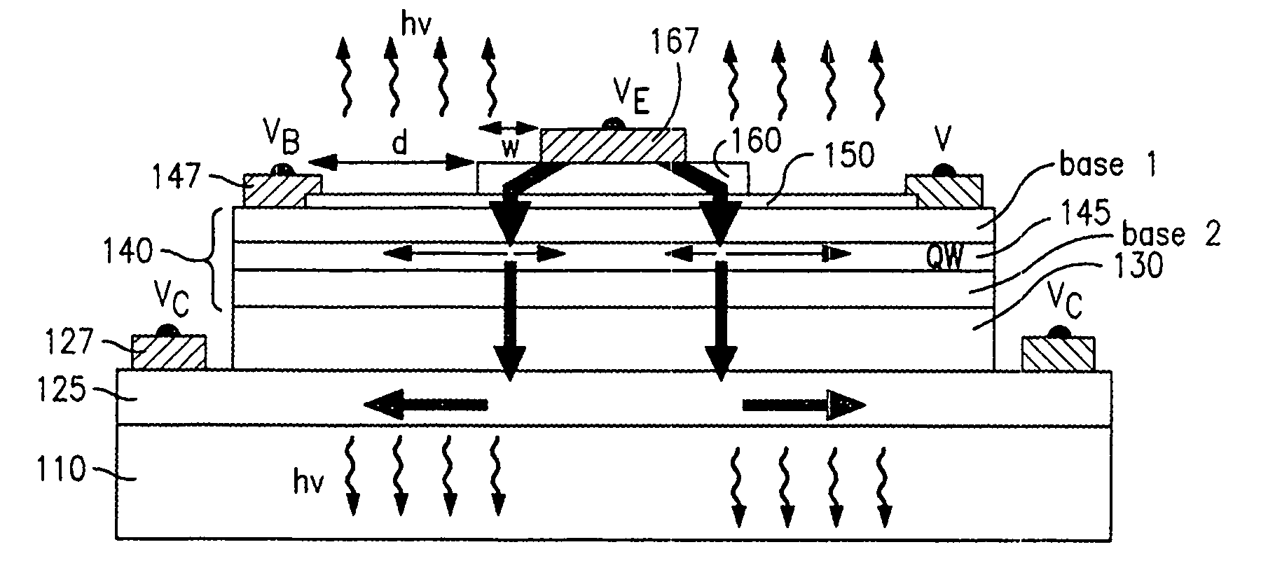
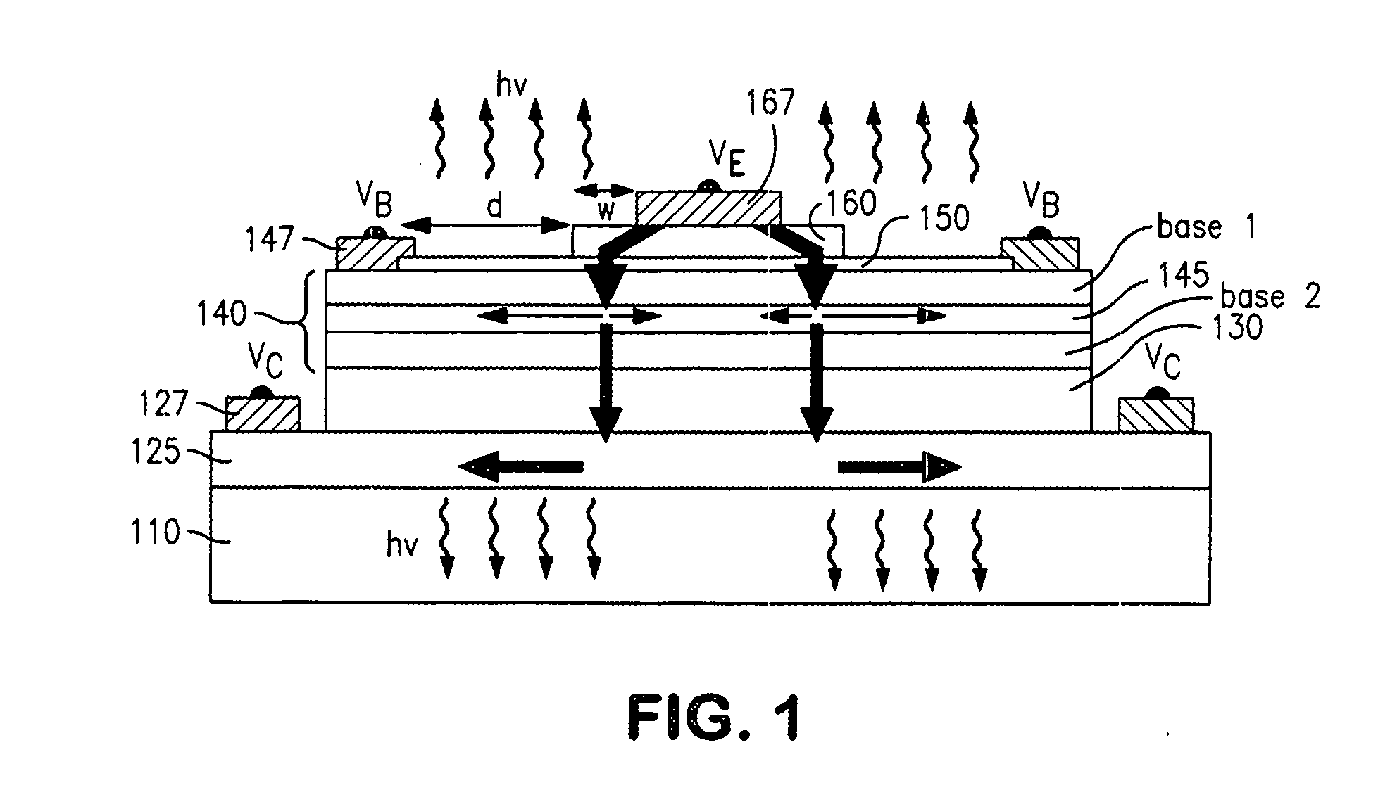
[0030]Referring to FIG. 1, there is shown a cross-sectional view of an optical tilted charge device, in the form of a light-emitting transistor, in accordance with an embodiment of the invention and which can be used in practicing an embodiment of the method of the invention. In FIG. 1, a subcollector region 125 is disposed on an undoped substrate 110. A mesa on subcollector 125 includes a base region 140 disposed between a collector region 130 and an emitter region 160 formed on a further mesa. The base region includes one or more quantum wells 145 between an upper base region (base 1) and a lower base region (base 2). In this embodiment, a collector electrode 127 contracts a surface of subcollector region 125, a base electrode 147 contacts a surface of base region 140, and an emitter electrode 167 contacts a surface of emitter region 160. A tunnel barrier layer 150 is disposed over the top surface of the base region 140, between the base region and emitter region 160, covering, in...


PUM


Abstract

A method for producing optical signals with improved efficiency, including the following steps: providing a layered semiconductor structure that includes a substrate, a semiconductor collector region of a first conductivity type, a semiconductor base region of a second conductivity type disposed on the collector region, and a semiconductor emitter region of the first semiconductor type disposed as a mesa over a portion of a surface of the base region; providing, in the base region, at least one region exhibiting quantum size effects; providing collector, base, and emitter electrodes, respectively coupled with the collector, base and emitter regions; providing a tunnel barrier layer over at least the exposed portion of the surface of the base region; and applying signals with respect to the collector, base, and emitter electrodes to produce optical signals from the base region.

Description

PRIORITY CLAIM[0001]Priority is claimed from U.S. Provisional Patent Application No. 61 / 629,175, filed Nov. 14, 2011, and said Provisional patent application is incorporated herein by reference.RELATED APPLICATION[0002]The subject matter of this application is related to subject matter of U.S. patent application Ser. No. ______, filed of even date herewith and assigned to the same assignee as the present application.FIELD OF THE INVENTION[0003]This invention relates to the field of semiconductor light emitting devices and techniques and, more particularly, to tilted charge light emitting devices and methods.BACKGROUND OF THE INVENTION[0004]Included in the background of the present invention are technologies relating to heterojunction bipolar transistors (HBTs, which are electrical tilted charge devices) and light-emitting transistors, transistor lasers, and tilted charge light-emitting diodes (respectively, LETs, TLs, and TCLEDs, all of which are optical tilted charge devices). A ti...

Claims


Application Information

Patent Timeline
IPC IPC(8): H01L33/06
CPCH01L33/06H01L33/38H01L33/0041
Inventor WALTER, GABRIEL
Owner QUANTUM ELECTRO OPTO SYST
Why Eureka
Try Eureka