Compositions and Methods for Texturing of Silicon Wafers

a technology of silicon wafers and compositions, applied in the field of texturing of the surface of silicon wafers, can solve the problems of low surface reflectivity, achieve the effects of reducing reflectivity, improving texturing uniformity, and reducing the reflectance of the textured surfa

Inactive Publication Date: 2013-05-23
VERSUM MATERIALS US LLC
View PDF18 Cites 30 Cited by
  • Summary
  • Abstract
  • Description
  • Claims
  • Application Information

AI Technical Summary

Benefits of technology

[0006]Compositions of this invention can be used to treat silicon wafers or substrates (the terms silicon wafers and substrates will be used interchangeably herein) in the texturing processes of this invention. The silicon wafers treated in accordance with these inventions may be used to make photovoltaic cells. Wafers subjected to compositions and / or methods of this invention may show improvement in the texturing uniformity and reduced reflectivity compared to the wafers not subjected to this treatment. Additional benefits that may be achieved with the method and / or composition of this invention may include one or more of the following: (1) the creation of uniform and smaller oval pits on the surface of the wafer with desirable Si loss; (2) decreased reflectance of the textured surface; and (3) consistent texturing results on silicon wafers from different suppliers.
[0007]It is desirable to have as low reflectivity as possible. Our invention provides compositions and methods to improve the texturing of the surface of the wafer. Our invention involves treating the wafer surface with a composition or compositions that comprises one or more surfactants in an acidic texturing solution. The composition modifies the wafer surface by creating smaller and uniform pits on the silicon wafer surface with desirable Si loss, resulting in improved uniformity of the textured surface that results in lower surface reflectivity.

Problems solved by technology

The composition modifies the wafer surface by creating smaller and uniform pits on the silicon wafer surface with desirable Si loss, resulting in improved uniformity of the textured surface that results in lower surface reflectivity.

Method used


Image

  • Compositions and Methods for Texturing of Silicon Wafers
  • Compositions and Methods for Texturing of Silicon Wafers
  • Compositions and Methods for Texturing of Silicon Wafers

Examples


example 1

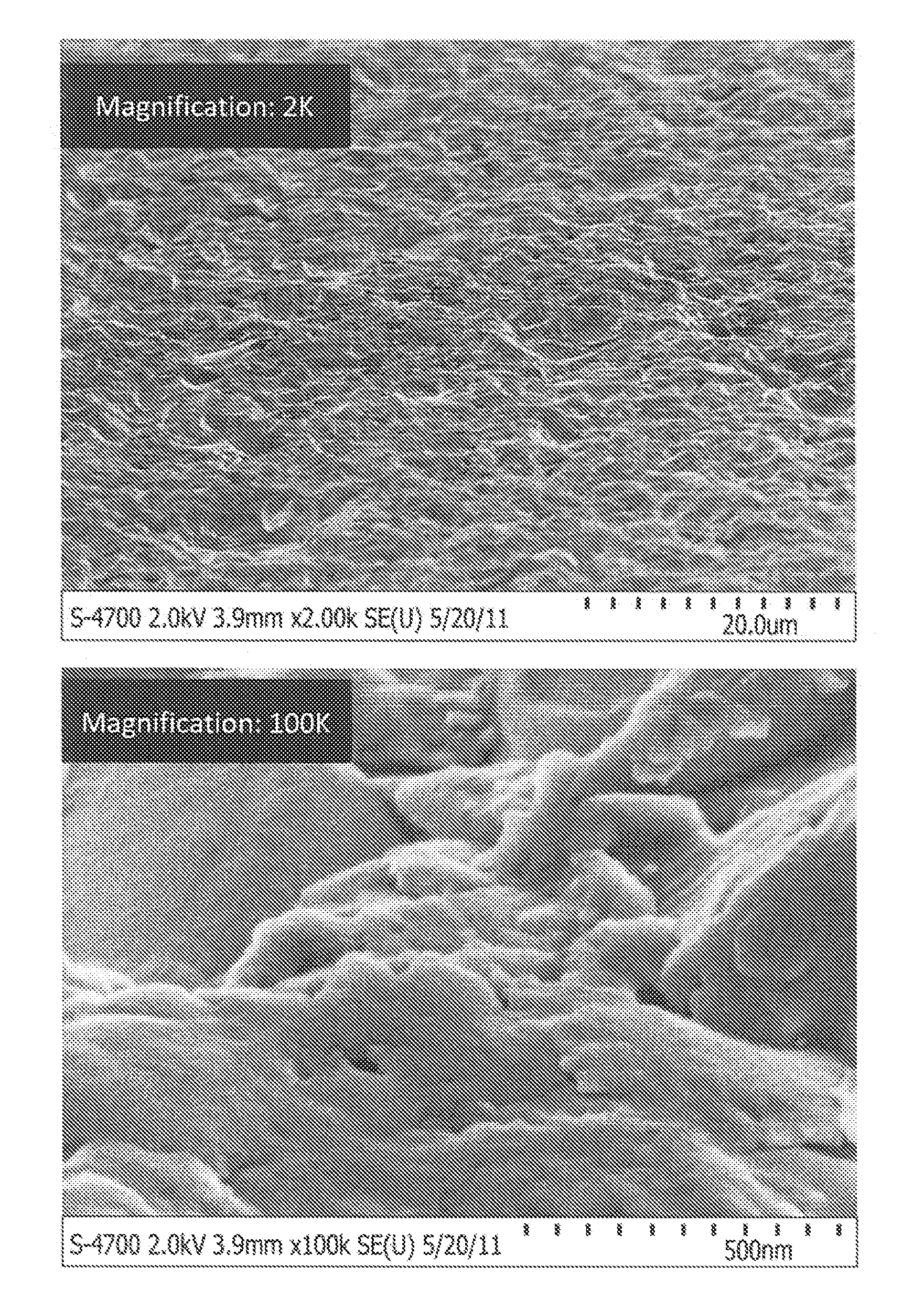
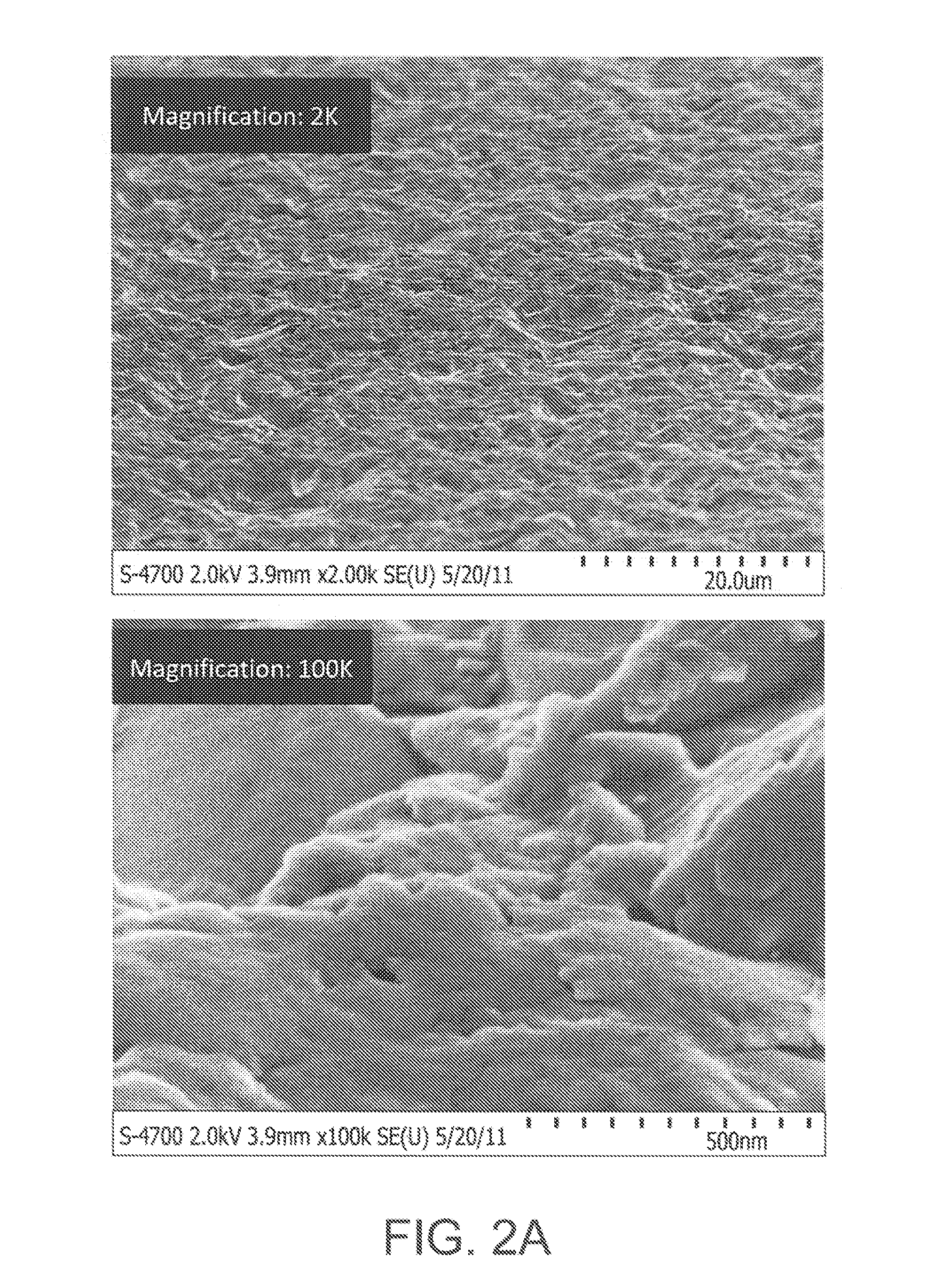
[0053]In this example, mono and multi-crystalline wafers (identified in the tables below were treated by a 2-step texturing process (with additional rinse and drying steps; however there were no saw damage nor other pre-treatment steps, e.g. no pre-clean steps)). The first texturing step entailed wetting by horizontally submerging each wafer into the first texturing composition identified in the tables below (Tables 1, 1A, 2, 2A, 3, 3A, 4, 4A, 5, 6 and 6A) for from about 1-3 min at 7-10° C., and then rinsing with deionized water (DIW) and nitrogen drying, followed by the second texturing step, of wetting by vertically submerging each treated wafer into a 0.5% to 5% by weight KOH aqueous solution (for nanopore removal) for 10 sec to 1 min at ambient temperature, and then rinsing each wafer with DIW and nitrogen drying the wafer. Silicon loses on both sides were determined based on weight changes. Reflectance was measured on each of the wafers, on the side of the wafer facing the bott...

example 2

[0058]Texturing composition Example F (Ex F) defined in Table 2A was used in the same 2 texturing steps process (with rinse and drying steps) as used in Example 1 and reported in Table 2 using different wafers from different wafer sources. The results are reported in Table 5.

TABLE 5WaferTTimeSi loss*WARsources(° C.)(min)μm400-1100 nm %wafer typesSource 17-81.56.1822.33%mono-Si7-81.54.4922.91%multi-SiSource 27-81.56.0223.41%mono-Si7-81.55.3722.20%multi-SiSource 37-81.54.2721.43%multi-SiSource 47-81.54.3323.68%multi-SiSource 57-81.54.4323.51%multi-Si*As described for Example 1, average-weighted reflectances were measured after step 104 F. (after wetting each wafer with 0.5 wt % KOH aqueous texturing solution at ambient temperature for 1 min).

example 3

[0059]Additional texturing compositions were tested in the same process described in Example 1. The results are reported in Table 6 (Note, three earlier examples are repeated in Table 6). Compositional information can be found for Comparative Ex 1 and Ex A in Table 1A and Comparative Ex II and Ex F in Table 2A.)

TABLE 6TexturingTTimeSi loss*WAR 400-waferCompositionsSurfactant(° C.)(min)μm1100 nm %typesComparativeNone7-813.9932.76%multi-SiEx IEx AHostapur ® SAS7-825.6225.15%multi-Si(10%)Ex O**Calfax ®DBA70 (10%)7-825.4725.24%multi-SiEx P***AEROSOL ®NPES -7-824.8022.09%multi-Si3030 P (30%)ComparativeNone7-815.4229.57%multi-SiEx IIEx FHostapur SAS (10%)7-81.56.1822.33%mono-SiEx QCalfax: DBA70 (10%)7-81.54.2523.57%multi-Si*As described for Example 1, average-weighted reflectance was measured after wetting each wafer with 0.5 wt % KOH aqueous texturing solution at ambient temperature for 1 min.**Calfax ®DBA70 (10%) is C12 (branched) diphenyl oxide disulfonic acid manufactured by Pilot Che...


PUM

PropertyMeasurementUnit
heightsaaaaaaaaaa
depthaaaaaaaaaa
wt %aaaaaaaaaa

Abstract

Texturing composition for texturing silicon wafers having one or more surfactants. Methods of texturing silicon wafers having the step of wetting said wafer with a texturing composition having one or more surfactants.

Description

CROSS-REFERENCE TO RELATED APPLICATIONS[0001]This Application claims the benefit of Provisional U.S. patent application Ser. No. 61 / 530,760 filed Sep. 2, 2011 (Attorney Docket No. 07482Z2), U.S. patent application Ser. No. 13 / 296836 filed Nov. 15, 2011 (Attorney Docket No. 07482Z2P) and U.S. application Ser. No. 61 / 416998 (Attorney Docket No. 07482Z) filed Nov. 24, 2010, all of which are incorporated by reference in their entirety.BACKGROUND OF THE INVENTION[0002]This invention relates to texturing of a surface of a silicon wafer. For improving the efficiency of conversion of light energy to electricity, a very low reflecting silicon surface is desired. For monocrystalline silicon for example, this is achieved by anisotropic etching of (100) Si wafers to form pyramid structures on the surface, in a process called as texturing. A uniform and dense distribution of pyramids is desired on the surface of the silicon wafer to achieve low reflectance. It is desired that the pyramid heights...

Claims


Application Information

Patent Timeline
Patent Type & Authority Applications(United States)
IPC IPC(8): H01L21/306
CPCH01L21/30604Y02E10/50H01L31/02363
Inventor WU, AIPINGRAO, MADHUKAR BHASKARATAMBOLI, DNYANESH CHANDRAKANT
Owner VERSUM MATERIALS US LLC
Why Eureka
Try Eureka