Semiconductor device and method for manufacturing same

a technology of semiconductors and semiconductors, applied in the direction of semiconductor devices, electrical devices, transistors, etc., can solve the problems of low efficiency in low current operations and increase in costs, and achieve the effects of preventing electric fields, reducing resistance, and increasing breakdown voltag

Active Publication Date: 2013-05-30
ROHM CO LTD
View PDF1 Cites 30 Cited by
  • Summary
  • Abstract
  • Description
  • Claims
  • Application Information

AI Technical Summary

Benefits of technology

[0016]With the super-junction structure, the depletion layer can be expanded in the direction along the boundary between the second conductive type column layer and the first conductive type base layer (that is, the thickness direction of the first conductive type base layer). As a result, it is possible to prevent electric fields from being concentrated in a localized area of the first conductive type base layer, thereby achieving a semiconductor device having a lower ON resistance and a higher breakdown voltage.
[0017]Further, in this semiconductor device, the first conductive type base layer receives electrons or holes from the second conductive type collector layer that is formed in a part of the rear surface portion of the first conductive type base layer, which allows the conductivity modulation to occur in the first conductive type base layer. As a result, in high current operations, the current can be raised in a manner similar to a current waveform of an IGBT.
[0018]That is, the semiconductor device of the present invention is equipped with an MOSFET that can reduce the ON resistance in low current operations and that can perform conductivity modulation in high current operations, allowing optimum device characteristics for desired applications.

Problems solved by technology

This results in a problem of low efficiency in low current operations when used in a driver circuit for a motor, for example.
However, in order to achieve MOSFETs that can be used in high current operations in addition to low current operations, the chip size of the MOSFETs needs to be larger, which causes an increase in cost.

Method used


Image

  • Semiconductor device and method for manufacturing same
  • Semiconductor device and method for manufacturing same
  • Semiconductor device and method for manufacturing same

Examples


working examples

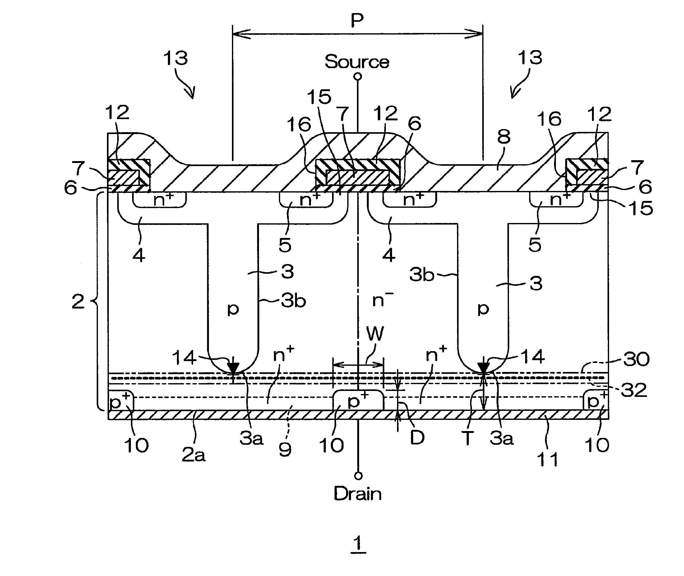
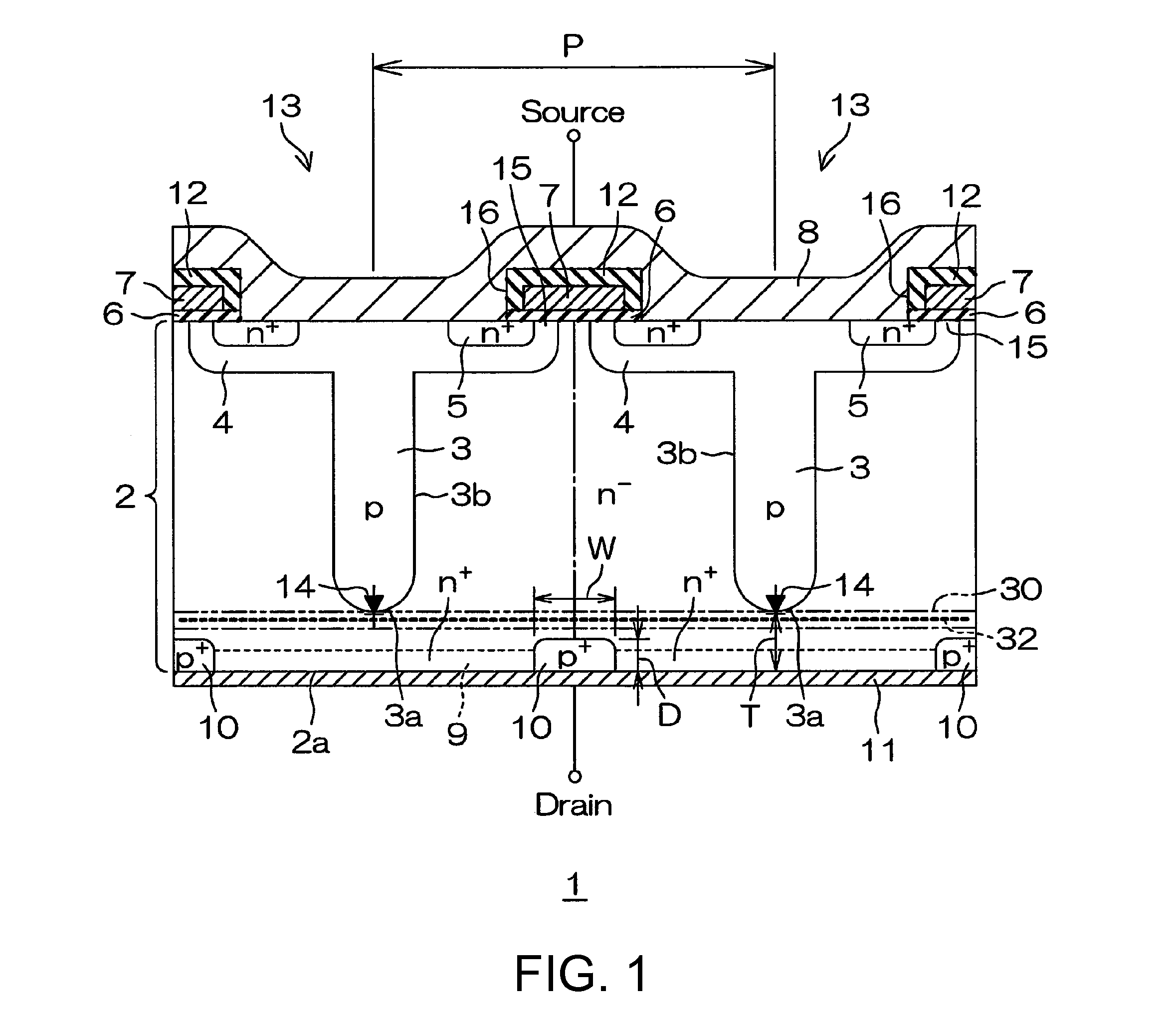
[0188]Next, simulations conducted to verify effects of certain aspects of the present invention will be explained. Simulations 1 to 3 below were conducted using semiconductor devices 1 that do not include the depletion layer stopper region 30 or the trap level region 32. As far as the simulated characteristics are concerned, these two regions do not substantively affect the results of Simulations 1 to 3.

[0189]In Simulation 1, the dependence of breakdown voltages on the thickness T of the n−-type base layer 2 immediately below the p-type column layer 3 was studied. In Simulation 1, a plurality of semiconductor devices 1 in which the thickness T of the n−-type base layer 2 immediately below the p-type column layer 3 was set to different values, i.e., 18 μm, 30 μm, and 40 μm, were prepared.

[0190]For each thickness T, five different samples were prepared. One sample is not provided with the p+-type collector layers 10 (no B ion implanted) and the other four samples are provided with the...


PUM


Abstract

A semiconductor device includes: an n-type base layer; a p-type base layer formed in a part of a front surface portion of the n-type base layer; an n+-type source layer formed in a part of a front surface portion of the p-type base layer; a gate insulating film formed on the front surface of the p-type base layer between the n+-type source layer and the n-type base layer; a gate electrode that faces the p-type base layer through the gate insulating film; a p-type column layer formed continuously from the p-type base layer in the n-type base layer; a p+-type collector layer formed in a part of a rear surface portion of the n-type base layer; a source electrode electrically connected to the n+-type source layer; and a drain electrode electrically connected to the n-type base layer and to the p+-type collector layer.

Description

[0001]This application is a continuation-in-part of PCT International Application No. PCT / JP2012 / 076482 designating the United States, filed on Oct. 12, 2012, which claims the benefit of Japanese Application No. 2011-227966, filed in Japan on Oct. 17, 2011. Both applications are hereby incorporated by reference in their entireties.[0002]The present application also claims the benefit of Japanese Application No. 2012-014415, filed in Japan on Jan. 26, 2012, which is hereby incorporated by reference in its entirety.BACKGROUND OF THE INVENTION[0003]1. Field of the Invention[0004]The present invention relates to a semiconductor device having a super-junction structure and a method of manufacturing the same.[0005]2. Description of Related Art[0006]IGBTs (insulated-gate bipolar transistors) and a conductivity modulation type MOSFET disclosed in Patent Document 1, for example, are known as switching elements that are used in an inverter circuit or a power circuit that is provided in home a...

Claims


Application Information

Patent Timeline
Patent Type & Authority Applications(United States)
IPC IPC(8): H01L29/739H01L29/66
CPCH01L29/66333H01L29/0696H01L2924/0002H01L29/7395H01L21/2605H01L2924/00
Inventor NAKAJIMA, TOSHIOHIGASHIDA, SYOJI
Owner ROHM CO LTD
Why Eureka
Try Eureka