Organic light-emitting diode including multi-layered hole transporting layer, and flat display device including the organic light-emitting diode

a light-emitting diode and multi-layer technology, applied in the direction of solid-state devices, thermoelectric devices, organic chemistry, etc., can solve the problems of low efficiency of formed devices and short lifespan (lifetime), and achieve the effect of improving the efficiency and lifespan of formed devices

Active Publication Date: 2013-06-06
SAMSUNG DISPLAY CO LTD
View PDF10 Cites 24 Cited by
  • Summary
  • Abstract
  • Description
  • Claims
  • Application Information

AI Technical Summary

Benefits of technology

[0008]An aspect of an embodiment of the present invention is directed toward an organic light-emitting diode including a multi-layered hole transporting layer that includes two different hole transporting compounds to improve the efficiency and lifespan (lifetime) of a formed device.

Problems solved by technology

However, charges are excessively injected and thus, a formed device may have low efficiency and a short lifespan (lifetime).

Method used


Image

  • Organic light-emitting diode including multi-layered hole transporting layer, and flat display device including the organic light-emitting diode
  • Organic light-emitting diode including multi-layered hole transporting layer, and flat display device including the organic light-emitting diode
  • Organic light-emitting diode including multi-layered hole transporting layer, and flat display device including the organic light-emitting diode

Examples


example 1

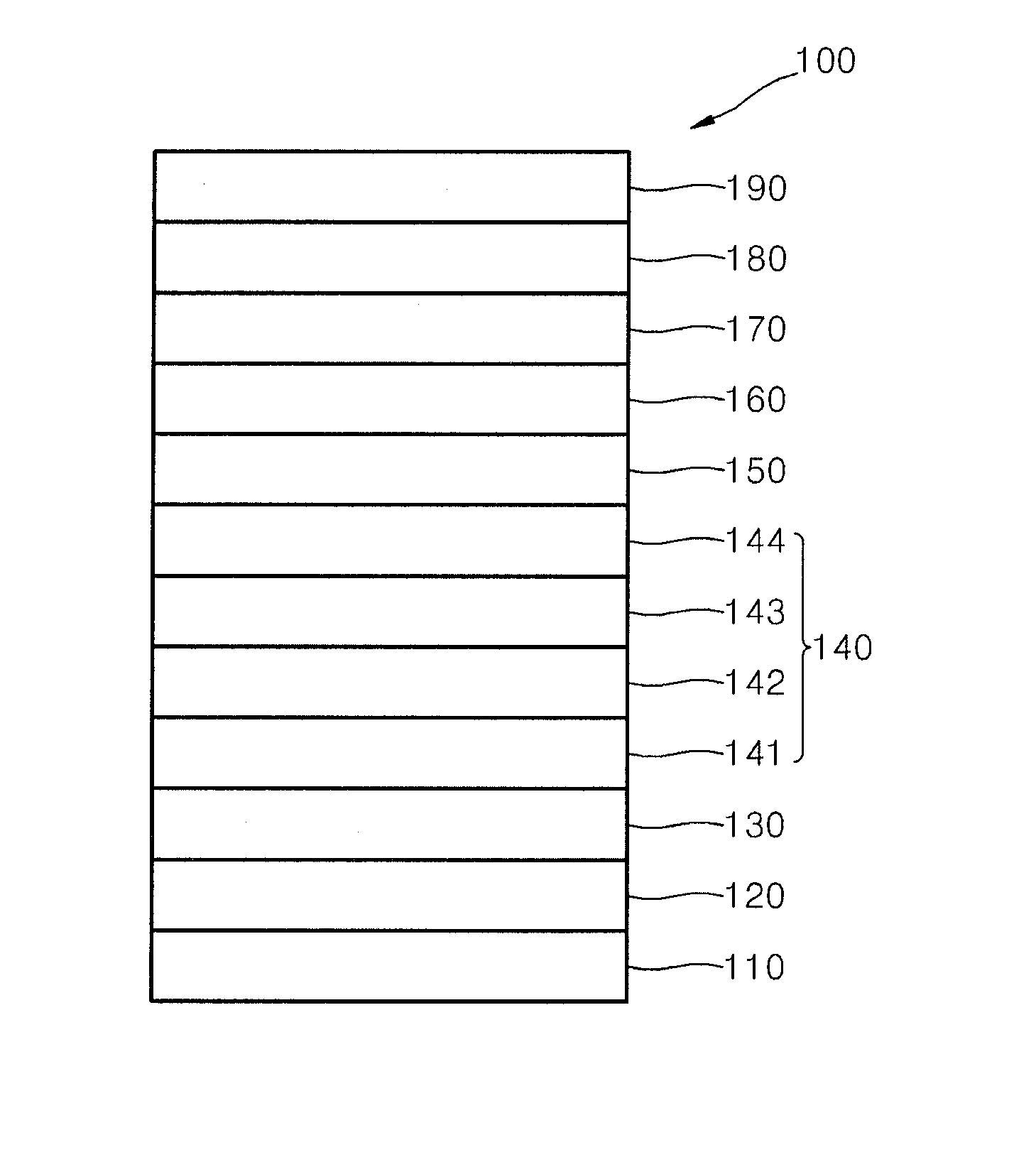
[0161]As an anode, 15 Ω / cm2(1200 Å) ITO glass substrate manufactured by Corning Co., Ltd was cut to a size of 50 mm×50 mm×0.7 mm and sonicated with isopropyl alcohol and pure water each for 5 minutes, and then an ultraviolet ray was irradiated thereto for 30 minutes, followed by exposure to ozone. Then, the resultant ITO glass substrate was installed in a vacuum deposition device.

[0162]Compound 301, Compound 35, and Compound 502 were vacuum co-deposited at a weight ratio of 60:40:1 on the ITO glass substrate to form a first charge generation layer having a thickness of 100 Å, and then Compound 301 and Compound 35 were vacuum co-deposited at a weight ratio of 60:40 on the first charge generation layer to form a first mixed layer having a thickness of 400 Å. Then, Compound 301, Compound 35, and Compound 502 were vacuum co-deposited at a weight ratio of 60:40:1 on the first mixed layer to form a second charge generation layer having a thickness of 100 Å, and then Compound 301 and Compo...

example 2

[0168]An organic light-emitting diode was manufactured in the same manner as in Example 1, except that when the first charge generation layer and the second charge generation layer were formed, Compound 301, Compound 35, and Compound 502 were used at a weight ratio of 70:30:1, and when the first mixed layer and the second mixed layer were formed, Compound 301 and Compound 35 were used at a weight ratio of 70:30.

example 3

[0169]An organic light-emitting diode was manufactured in the same manner as in Example 1, except that when the first charge generation layer and the second charge generation layer were formed, Compound 301, Compound 35, and Compound 502 were used at a weight ratio of 70:30:3, and when the first mixed layer and the second mixed layer were formed, Compound 301 and Compound 35 were used at a weight ratio of 70:30.


PUM


Abstract

An organic light-emitting diode including: a first mixed layer between an emission layer and a first electrode and including first and second compounds; a second mixed layer between the emission layer and the first mixed layer and including third and fourth compounds; a first charge generation layer between the first mixed layer and the first electrode and including the first and second compounds and a first charge generation material; a second charge generation layer between the first mixed layer and the second mixed layer and including the third and fourth compounds and a second charge generation material; and a buffer layer between the emission layer and the second mixed layer, the first and the third compounds are each independently a compound represented by Formula 1 below, and the second compound and fourth compounds are each independently a compound represented by Formula 2 below:

Description

CROSS-REFERENCE TO RELATED PATENT APPLICATION[0001]This application claims priority to and the benefit of Korean Patent Application No. 10-2011-0128526, filed on Dec. 2, 2011, in the Korean Intellectual Property Office, the disclosure of which is incorporated herein in its entirety by reference.BACKGROUND[0002]1. Field[0003]The following description relates to an organic light-emitting diode including a multi-layered hole transporting layer and a flat display device including the organic light-emitting diode.[0004]2. Description of Related Art[0005]Organic light emitting diodes are self-emission devices and enable generation of multi-color images. In addition, the organic light emitting diodes have a wide viewing angle, a high contrast ratio, a short response time, and excellent brightness, driving voltage, and response speed characteristics.[0006]In a typical organic light-emitting diode, an anode is formed on a substrate, and a hole transport layer, an emission layer, an electron ...

Claims


Application Information

Patent Timeline
Patent Type & Authority Applications(United States)
IPC IPC(8): H01L51/54
CPCH01L51/50H01L27/32H01L51/5064H01L51/0061H01L51/0067H01L51/006C07D209/86C07D403/12C07D401/14C07D401/12H10K85/636H10K85/633H10K85/654H10K50/156C07D209/82H10K85/631H10K85/6572
Inventor KHO, SAM-ILPARK, MIE-HWAJEONG, HYE-INKWAK, YOON-HYUNSHIN, DAE-YUPLEE, KWAN-HEE
Owner SAMSUNG DISPLAY CO LTD
Why Eureka
Try Eureka