Check patentability & draft patents in minutes with Patsnap Eureka AI!

Semiconductor memory device and method of operating the same

a memory device and semiconductor technology, applied in the field of semiconductor memory devices and a method of operating the same, can solve the problems of excessive electric field applied to an insulating layer, further deterioration of the characteristics of the insulating layer, so as to minimize the stress of memory cells during operations

Active Publication Date: 2013-06-06
SK HYNIX INC
View PDF5 Cites 4 Cited by
  • Summary
  • Abstract
  • Description
  • Claims
  • Application Information

AI Technical Summary

Benefits of technology

This patent is about a semiconductor memory device and a way to operate it that lessens stress on memory cells during operations. The technical effect is that this reduces wear and tear on the memory cells, which results in better performance and reliability.

Problems solved by technology

As a result, an excessive electric field may be applied to an insulating layer (for example, a tunnel insulating layer or a dielectric layer) included in the memory cell.
As a result, characteristics of the insulating layer may be deteriorated.
In addition, with increasing cumulative numbers of program operations and erase operations, if a higher erase voltage is supplied to compensate for deterioration of erase characteristics, the characteristics of the insulating layers may be further deteriorated.

Method used


Image

  • Semiconductor memory device and method of operating the same
  • Semiconductor memory device and method of operating the same
  • Semiconductor memory device and method of operating the same

Examples


Embodiment Construction

[0018]Hereinafter, various embodiments will be described in detail with reference to the accompanying drawings. The figures are provided to allow those having ordinary skill in the art to understand the scope of the embodiments of the disclosure. The present invention may, however, be embodied in different forms and should not be construed as limited to the embodiments set forth herein. Rather, these embodiments are provided so that this disclosure will be thorough and complete, and will fully convey the scope of the present invention to those skilled in the art.

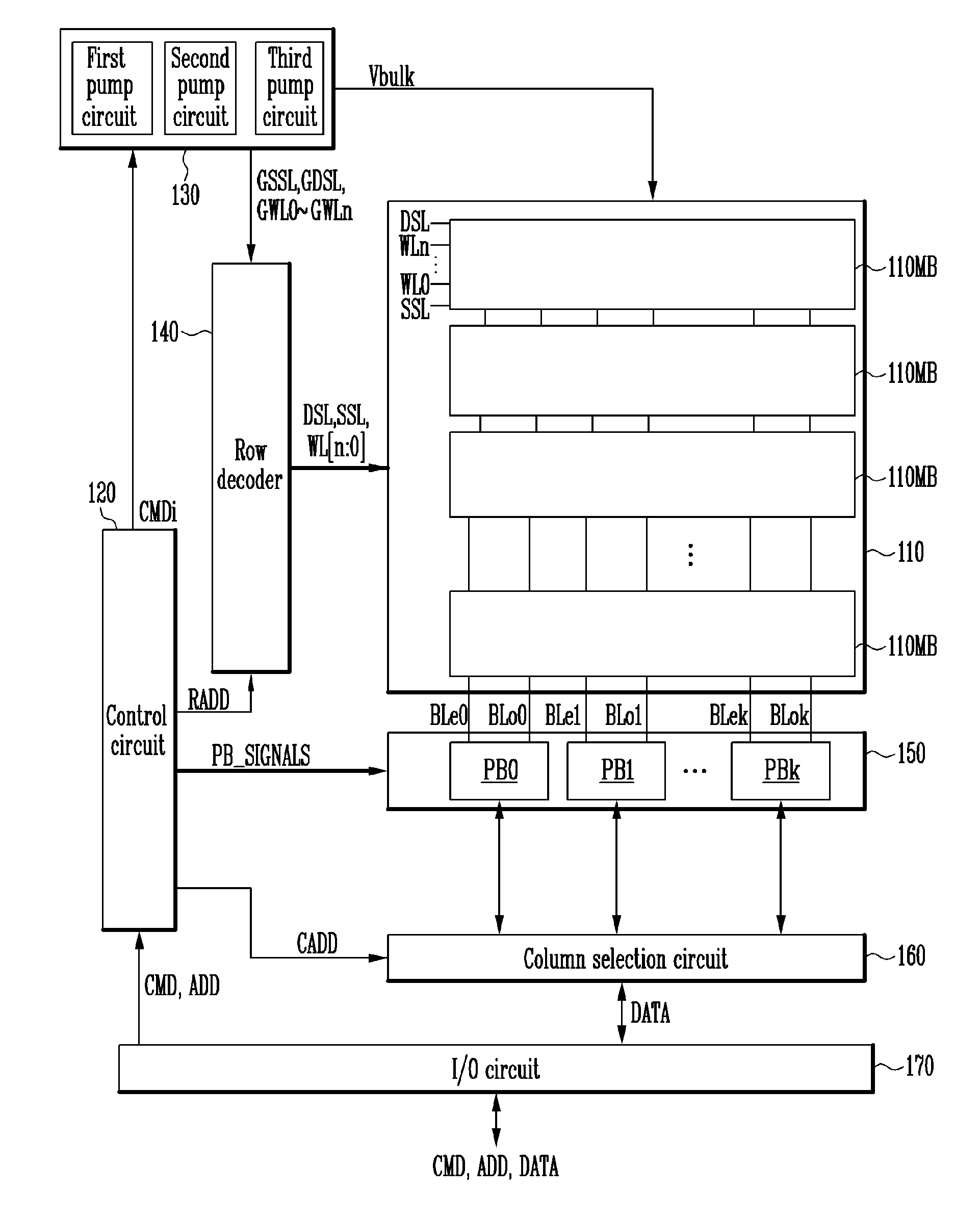
[0019]FIG. 1 is a circuit diagram of a semiconductor memory device according to an embodiment.

[0020]Referring to FIG. 1, the semiconductor memory device may include a memory array 110 and peripheral circuits 120 to 170. The memory array 110 may include a plurality of memory cells, which may be grouped in memory blocks. The peripheral circuits 120 to 170 may include a control circuit 120, a voltage generation circuit 130, a r...


PUM


Abstract

A semiconductor memory device includes a memory array including a plurality of memory cells, and a peripheral circuit configured to perform an erase operation by supplying a first erase voltage to selected memory cells and perform an erase verify operation by supplying an erase verify voltage to the selected memory cells, wherein the peripheral circuit is configured to increase the first erase voltage to a first level at a first rising rate for a first rising period and increase the first erase voltage to a first target level at a second rising rate lower than the first rising rate for a second rising period.

Description

[0001]The present application claims priority to Korean patent application number 10-2011-0129677 filed on Dec. 6, 2011, in the Korean Intellectual Property Office, the entire disclosure of which is incorporated by reference herein.BACKGROUND[0002]1. Technical Field[0003]Various embodiments relate generally to a semiconductor memory device and a method of operating the same and, more particularly, to a semiconductor memory device including memory cells and a method of operating the same.[0004]2. Related Art[0005]A semiconductor memory device includes a memory array. The memory array includes a plurality of memory cells. Connection relationships and arrangements of memory cells vary depending on types of memory devices. For example, in a NAND flash memory device, memory cells are coupled in series between bit lines and a source line.[0006]An operating voltage is to be supplied to memory cells in order to store data in the memory cells, output data stored in the memory cells or erase ...

Claims


Application Information

Patent Timeline
IPC IPC(8): G11C16/04
CPCG11C16/3445G11C16/16G11C16/04G11C16/0483G11C7/10G11C16/14G11C16/34
Inventor PARK, NOH YONGKIM, HYUNG SEOK
Owner SK HYNIX INC
Features
  • R&D
  • Intellectual Property
  • Life Sciences
  • Materials
  • Tech Scout
  • Unparalleled Data Quality
  • Higher Quality Content
  • 60% Fewer Hallucinations
Learn More