Pixel structure of electroluminescent display panel

a technology of electroluminescent display panel and pixel structure, which is applied in the direction of instruments, semiconductor devices, organic light emitting devices, etc., can solve the problems of difficult to further improve the aperture ratio and resolution of a conventional electroluminescent display panel, distance limitation between adjacent openings of fine metal masks, etc., to avoid light-mixing problems and improve aperture ratio and resolution.

Active Publication Date: 2013-06-13
AU OPTRONICS CORP
View PDF2 Cites 30 Cited by
  • Summary
  • Abstract
  • Description
  • Claims
  • Application Information

AI Technical Summary

Benefits of technology

[0005]It is therefore one of the objectives of the present invention to provide a pixel structure of an electroluminescent display panel for avoiding light-mixing problem occurred between adjacent sub-pixel regions with different colors and for raising the aperture ratio and resolution.

Problems solved by technology

However, there exists a distance limitation between the adjacent openings of the fine metal mask, and there has to be disposed certain spacing between adjacent sub-pixel regions of different colors in order to avoid light mixing between adjacent sub-pixel regions that generate different colors of light.
Therefore, it is hard to further improve the aperture ratio and resolution of a conventional electroluminescent display panel.

Method used


Image

  • Pixel structure of electroluminescent display panel
  • Pixel structure of electroluminescent display panel
  • Pixel structure of electroluminescent display panel

Examples


Embodiment Construction

[0015]To provide a better understanding of the present invention to the skilled users in the technology of the present invention, preferred embodiments will be detailed as follows. The preferred embodiments of the present invention are illustrated in the accompanying drawings with numbered elements to elaborate the contents and effects to be achieved.

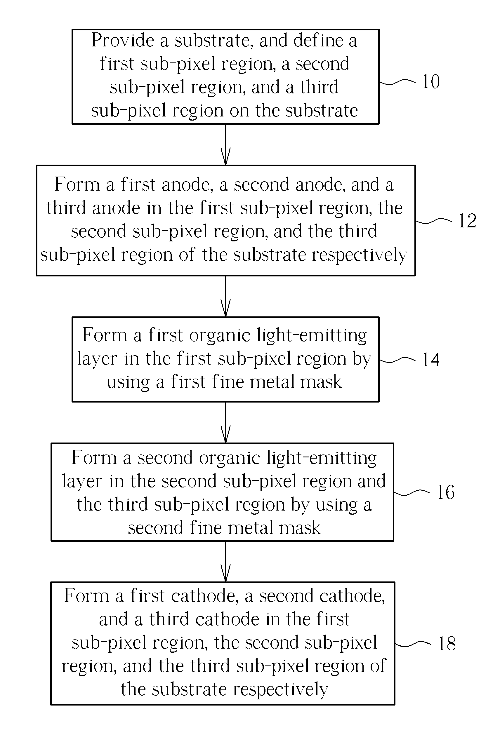
[0016]With reference to FIG. 1, FIG. 1 is a process flow diagram of a fabrication method of a pixel structure of an electroluminescent display panel of the present invention. As shown in FIG. 1, the fabrication method of a pixel structure of an electroluminescent display panel of the present invention mainly includes the following steps:

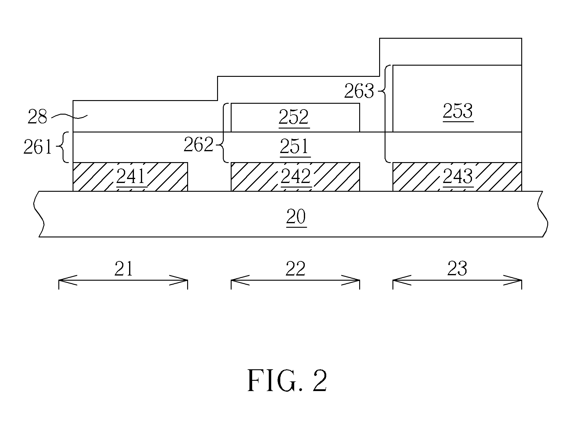
[0017]Step 10: Provide a substrate, and define a first sub-pixel region, a second sub-pixel region, and a third sub-pixel region on the substrate;

[0018]Step 12: Respectively form a first anode, a second anode, and a third anode in the first sub-pixel region, the second sub-pixel region, and the third sub...


PUM

PropertyMeasurementUnit
of wavelengthaaaaaaaaaa
cavity lengthsaaaaaaaaaa
thicknessesaaaaaaaaaa

Abstract

A pixel structure of electroluminescent display panel has a first sub-pixel region, a second sub-pixel region, and a third sub-pixel region. The pixel structure of electroluminescent display panel includes a first organic light-emitting layer, and a second organic light-emitting layer. The first organic light-emitting layer is disposed in the first sub-pixel region for generating a first primary color light in the first sub-pixel region. The second organic light-emitting layer is disposed in the second sub-pixel region, and the third sub-pixel region for generating a second primary color light in the second sub-pixel region, and for generating a third primary color light in the third sub-pixel region. The first sub-pixel region, the second sub-pixel region, and the third sub-pixel region have different cavity lengths.

Description

BACKGROUND OF THE INVENTION[0001]1. Field of the Invention[0002]The present invention relates to a pixel structure of an electroluminescent display panel, and a fabrication method thereof, and more particularly, to a pixel structure of an electroluminescent display panel having a common organic light-emitting layer formed in two adjacent sub-pixel regions for displaying different primary color lights, and a fabrication method thereof.[0003]2. Description of the Prior Art[0004]Due to its self-luminous, high contrast ratio, compact size, and wide viewing angle properties, electroluminescent display panel e.g. organic light-emitting diode (OLED) display panel has been expected to prevail in the display market of next generation. The organic light-emitting layer used in a conventional electroluminescent display panel is formed through an evaporation process by using a fine metal mask (FMM). However, there exists a distance limitation between the adjacent openings of the fine metal mask,...

Claims


Application Information

Patent Timeline
Patent Type & Authority Applications(United States)
IPC IPC(8): G09G3/30
CPCG09G3/30H01L51/5088H01L51/5265Y10T29/49002H01L51/56H01L2251/56H01L27/3206H10K59/30H10K50/17H10K50/852H10K71/00
Inventor LIU, MENG-YULIU, CHIH-CHEHSU, SHIH-FENG
Owner AU OPTRONICS CORP
Why Eureka
Try Eureka