Solder ball device, housing having a solder ball device and production process for a solder ball device

a technology of solder ball and solder ball, which is applied in the direction of soldering devices, manufacturing tools, and capacitors, etc., can solve the problems of limiting cracking of the solder ball connection, and reducing the service life of the bga, so as to reduce the mechanical stress

Inactive Publication Date: 2013-06-27
ROBERT BOSCH GMBH
View PDF8 Cites 0 Cited by
  • Summary
  • Abstract
  • Description
  • Claims
  • Application Information

AI Technical Summary

Benefits of technology

[0006]An objective of the present invention is the reduction in the mechanical stresses on the soldered connection of the BGA and on the circuit components on the inside.

Problems solved by technology

The bigger the BGA, the more mechanical stresses between the BGA and the printed-circuit board limit the service life of the BGA.
In particular, but not only, the different thermal expansion coefficients of the BGA and the printed-circuit board cause mechanical tensions in response to temperature changes, which may, for instance, allow the soldering connection, usually the solder balls, to crack.

Method used


Image

  • Solder ball device, housing having a solder ball device and production process for a solder ball device
  • Solder ball device, housing having a solder ball device and production process for a solder ball device
  • Solder ball device, housing having a solder ball device and production process for a solder ball device

Examples


Embodiment Construction

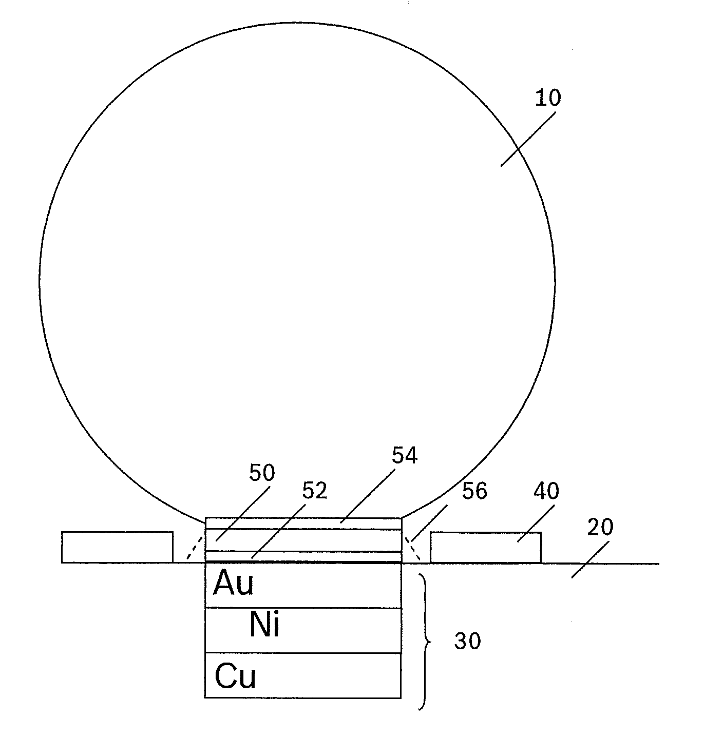
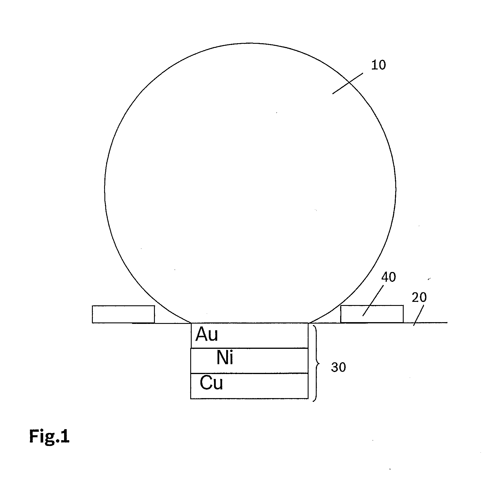
[0019]FIG. 1 shows the solder ball device of the related art. A cutout of a BGA is shown schematically having a laminate 20 that has a contact surface 30, and having a solder ball 10, which is situated on contact surface 30 in an electrically contacting manner. Contact surface 30 is a metallic contact surface and, in this exemplary embodiment, has a sequence of metallic layers of copper (Cu), nickel (Ni) and gold (Au), the solder ball being connected to the gold layer. Solder ball 10 is composed, for example, of SnAgCu or SnPb. The planar extension of the connection of solder ball 10 to BGA 20 is bordered either by a mask made of solder stop lacquer 40 (“solder mask defined”), or such a mechanical contact is specifically avoided (non-solder mask defined”).

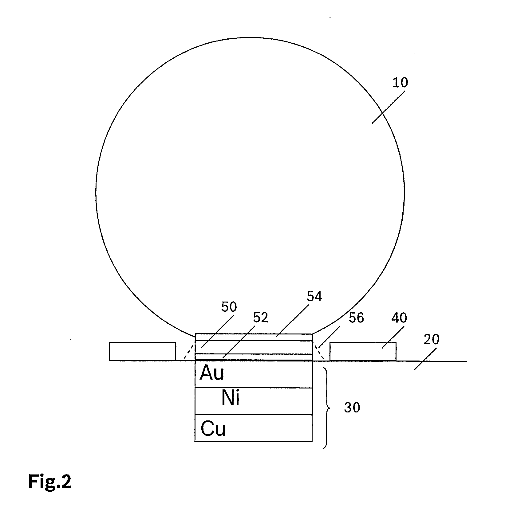
[0020]FIG. 2 shows a solder ball device according to the present invention. In contrast to the related art, an electric, conductive polymer 50 is situated between solder ball 10 and contact surface 30. An epoxy filled with silver (...


PUM

PropertyMeasurementUnit
conductiveaaaaaaaaaa
adhesionaaaaaaaaaa
mechanical stressesaaaaaaaaaa

Abstract

A solder ball device has a contact surface and a solder ball that is connected electrically conductively to the contact surface. Between the solder ball and the contact surface, a conductive polymer is situated, which is connected to the solder ball and the contact surface.

Description

BACKGROUND OF THE INVENTION[0001]1. Field of the Invention[0002]The present invention relates to a solder ball device, a housing having a solder ball device, as well as a production method for a solder ball device.[0003]2. Description of the Related Art[0004]Housings having solder ball devices (also known as ball grid arrays, “BGA”) have been used for a long time as packaging for electronic circuits. In this context, according to the standard, the Si circuits (ASIC, etc.) are adhered to an epoxy laminate and are wire-bonded. The laminate is comparable to a very thin printed-circuit board. Besides the mechanical fixing of the Si circuits, it also produces the electrical connections between the wire bonds of the Si circuits and the contact surfaces on the underside of the laminate. As protection from external influences, and for improved further processing, the Si circuits including the wire bonds are encased by extrusion, the laminate continuing to provide the underside of the BGA. F...

Claims


Application Information

Patent Timeline
Patent Type & Authority Applications(United States)
IPC IPC(8): H01B1/20H01B13/30
CPCH01L2924/1461H01L2224/13H01B1/20H01B13/30H01L2924/00
Inventor ROJAHN, ROBERT
Owner ROBERT BOSCH GMBH
Why Eureka
Try Eureka