Semiconductor device and fabricating method thereof

Active Publication Date: 2013-06-27
UNITED MICROELECTRONICS CORP
View PDF1 Cites 32 Cited by
  • Summary
  • Abstract
  • Description
  • Claims
  • Application Information

AI Technical Summary

Benefits of technology

[0012]In the present invention, the metal gate structure may avoid being damaged during the formation of the contact holes because the replacement metal gate process is completed after forming

Problems solved by technology

With the trend towards scaling down the size of semiconductor devices, conventional poly-silicon gates face problems such as boron penetration and unavoidable depletion effect leading to inferior performances.
Because of these problems, the equivalent thickness of the gate dielectric layer increases, reducing the gate capacitance, and lowering a driving force of the devices.
After performing the ann

Method used


Image

  • Semiconductor device and fabricating method thereof
  • Semiconductor device and fabricating method thereof
  • Semiconductor device and fabricating method thereof

Examples


Example

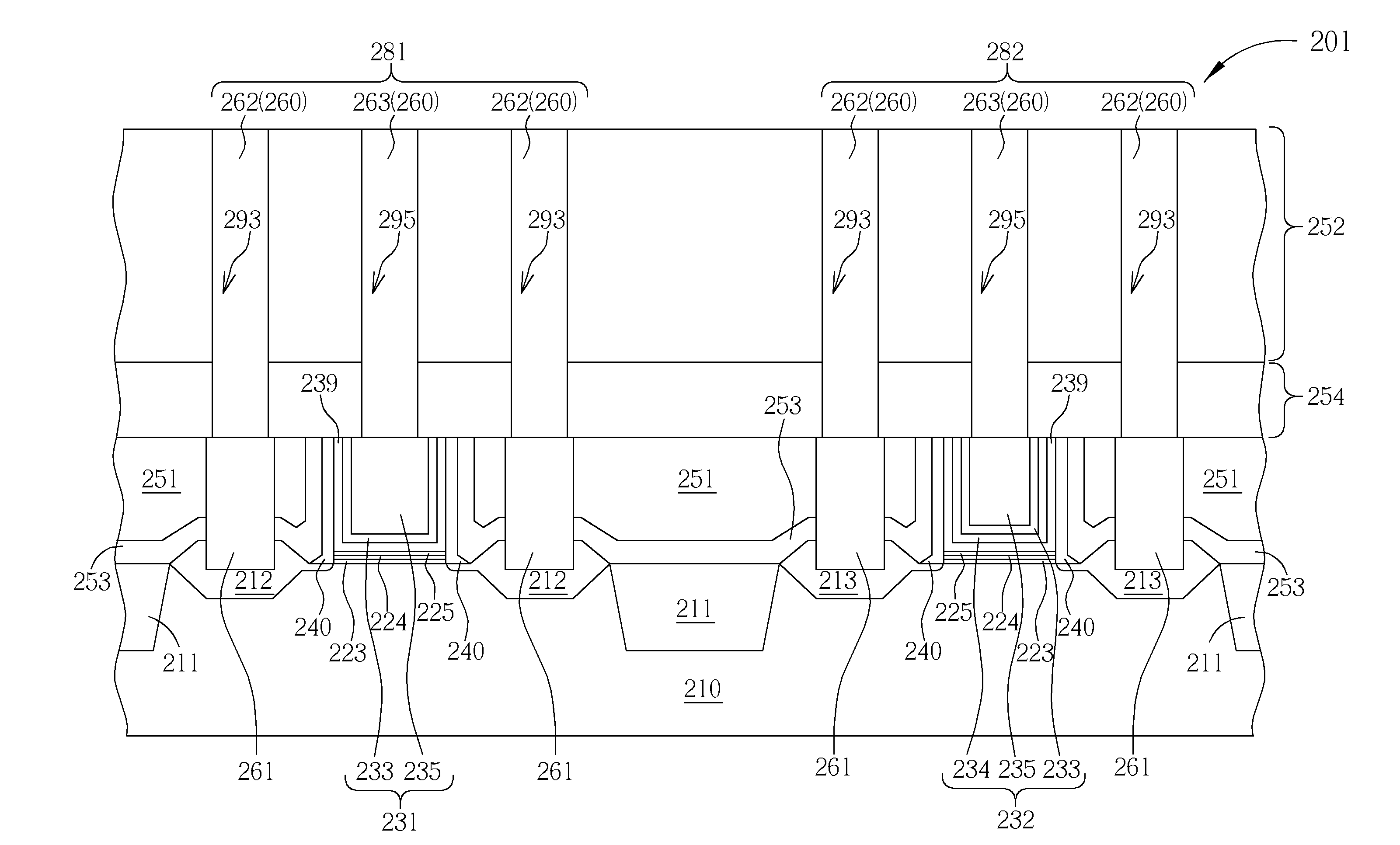
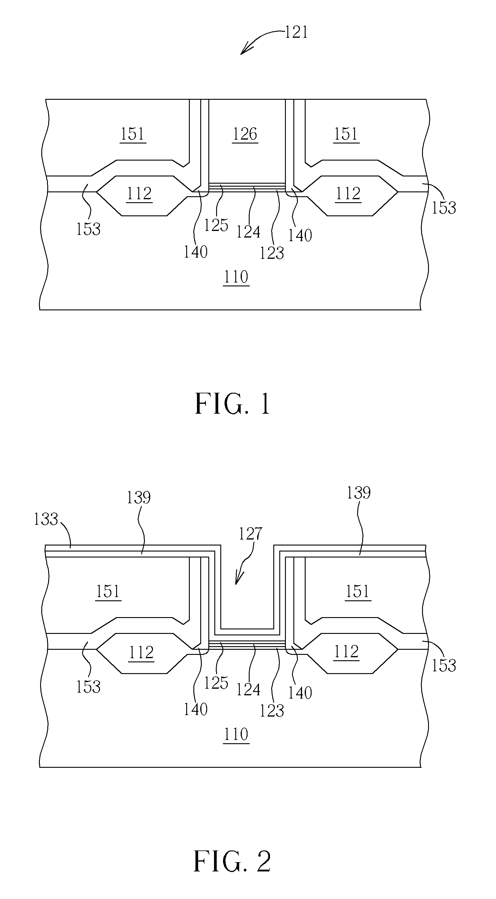
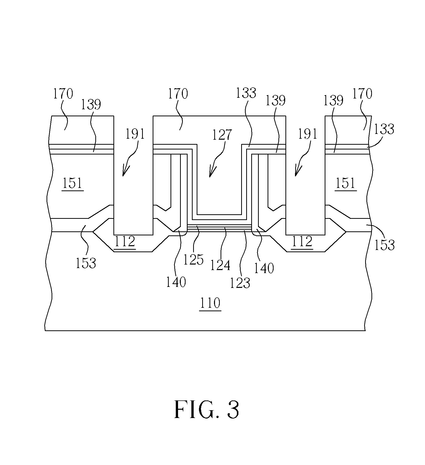
[0016]Please refer to FIGS. 1-5. FIGS. 1-5 are schematic diagrams illustrating a manufacturing method of the semiconductor device according to the first preferred embodiment of the present invention. The manufacturing method of the semiconductor device in this embodiment includes the following steps. First, as shown in FIG. 1, a substrate 110 is provided. A sacrificial gate structure 121 is formed on the substrate 110, a doping region 112 is formed in the substrate 110 at both sides of the sacrificial gate structure 121, and a first ILD layer 151 is formed to cover the doping region 112. In this embodiment, the sacrificial gate structure 121 may include a high dielectric constant (high-k) gate dielectric layer 124 and a sacrificial gate material layer 126 such as a poly-silicon material layer. The high-k gate dielectric layer 124 may be formed between the substrate 110 and the sacrificial gate material layer 126. Additionally, in this embodiment, a spacer 140 may be formed on both s...


PUM


Abstract

A manufacturing method of a semiconductor device includes the following steps. First, a substrate is provided. At least one gate trench and a first inter-layer dielectric layer are formed on the substrate. A work function metallic layer is then formed in the gate trench. A first contact hole is then formed in the first inter-layer dielectric layer. A main conductive layer is formed in the gate trench and the first contact hole simultaneously.

Description

BACKGROUND OF THE INVENTION[0001]1. Field of the Invention[0002]The present invention relates to a semiconductor device and a manufacturing method thereof, more particularly to a semiconductor device and a manufacturing method thereof wherein a contact hole is formed on a doping region before forming a metal gate structure.[0003]2. Description of the Prior Art[0004]Poly-silicon is conventionally used as a gate electrode in semiconductor devices, such as metal-oxide-semiconductors (MOS). With the trend towards scaling down the size of semiconductor devices, conventional poly-silicon gates face problems such as boron penetration and unavoidable depletion effect leading to inferior performances. Because of these problems, the equivalent thickness of the gate dielectric layer increases, reducing the gate capacitance, and lowering a driving force of the devices. Therefore, work function metals that are suitable for use as high dielectric constant (high-k) gate dielectric layers are emplo...

Claims


Application Information

Patent Timeline
IPC IPC(8): H01L21/283H01L27/092
CPCH01L21/823807H01L21/823814H01L21/823842H01L21/823871H01L21/76897H01L29/517H01L29/66545H01L29/7834H01L29/4966H01L23/485H01L23/5226H01L21/76805
Inventor SU, HAOHU, HANGLIAO, HONG
Owner UNITED MICROELECTRONICS CORP
Why Eureka
Try Eureka