NAND type non-volatile memory and operating method thereof

Inactive Publication Date: 2009-09-24
POWERCHIP SEMICON CORP
View PDF4 Cites 8 Cited by
  • Summary
  • Abstract
  • Description
  • Claims
  • Application Information

AI Technical Summary

Benefits of technology

[0021]In a NAND type non-volatile memory provided by the present invention, a dummy memory cell row and a dummy bit line are directly served as a current path for connecting a source line. Accordingly, no additional fabrication process is required for fabricating the source line plug and the memory array has a regular pattern. As a result, the process window of photolithography and etching process is improved.
[0022]In a NAND type non-volatile memory provided by the present invention, only the space of a dummy bit line served as a current path for conne

Problems solved by technology

Because the source line plug takes up at least part of the surface area of the (at least three) bit

Method used


Image

  • NAND type non-volatile memory and operating method thereof
  • NAND type non-volatile memory and operating method thereof
  • NAND type non-volatile memory and operating method thereof

Examples


Example

[0030]Reference will now be made in detail to the present preferred embodiments of the invention, examples of which are illustrated in the accompanying drawings. Wherever possible, the same reference numbers are used in the drawings and the description to refer to the same or like parts.

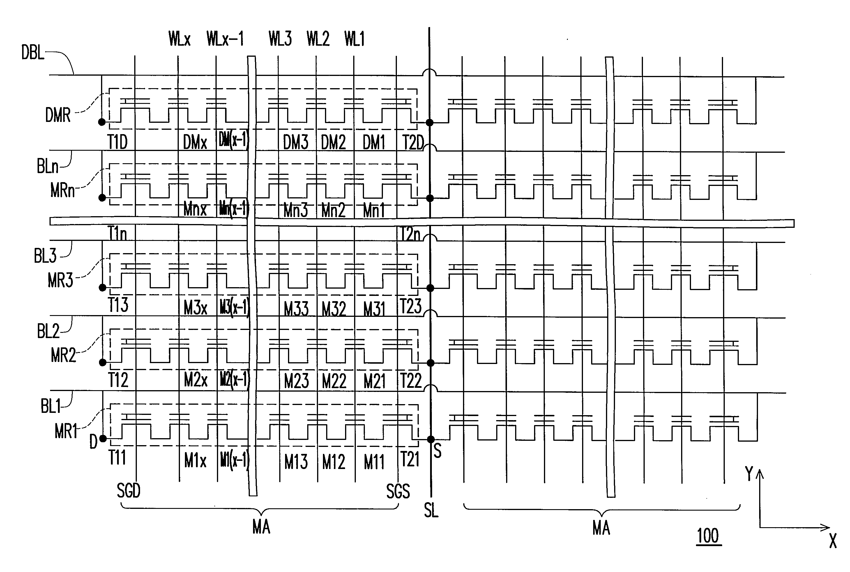
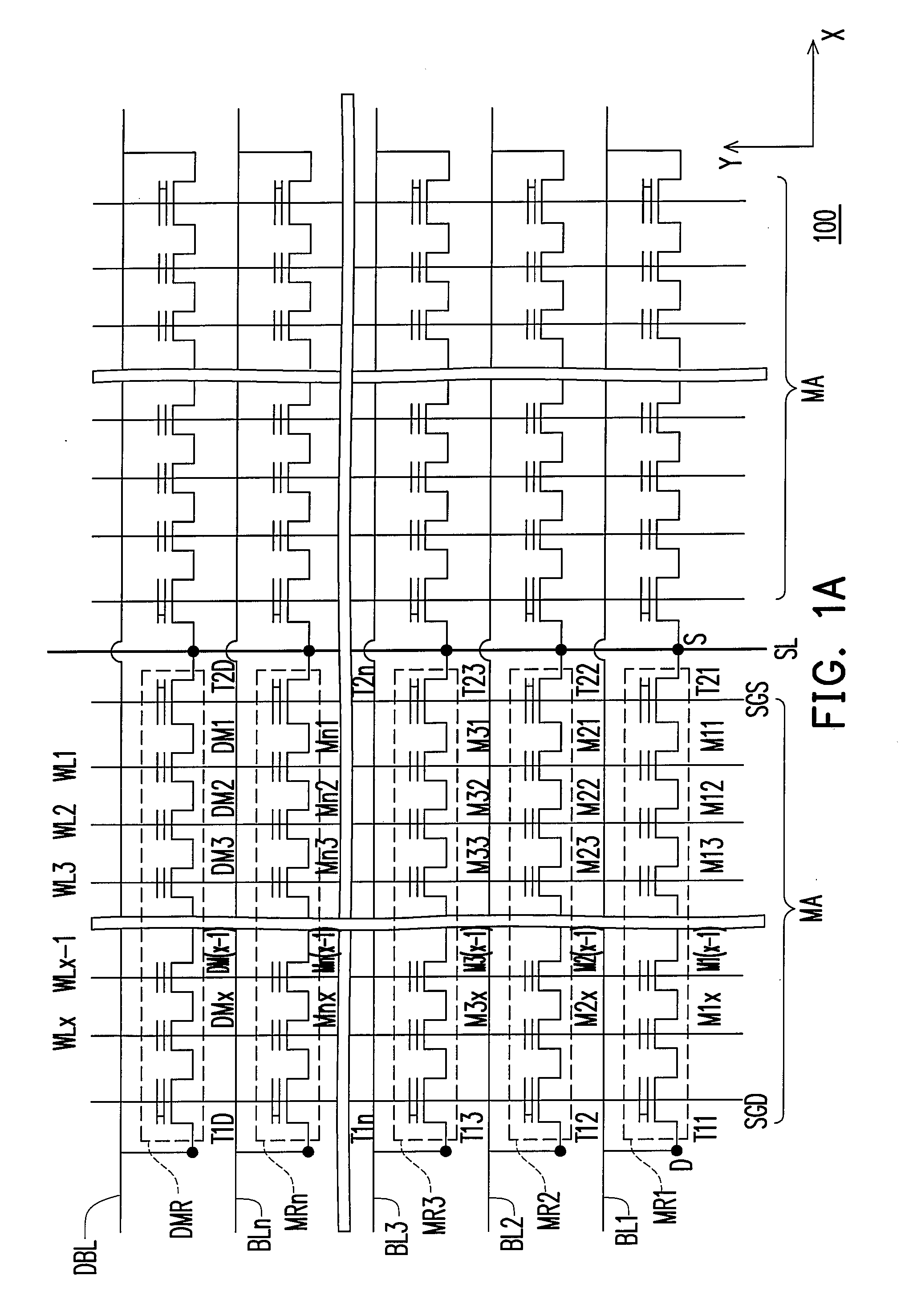
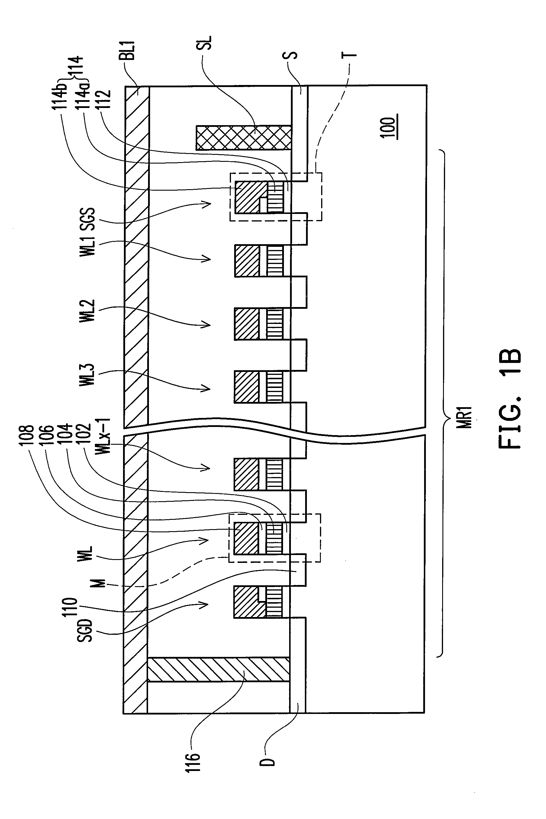
[0031]FIG. 1A is a schematic circuit diagram of a NAND type non-volatile memory according to an embodiment of the present invention. FIG. 1B is a cross-sectional view of a NAND type non-volatile memory according to an embodiment of the present invention.

[0032]Referring to FIG. 1A and FIG. 1B, the NAND type non-volatile memory provided by the present invention may be composed of a plurality of memory cell arrays MA. The memory cell arrays MA will be described below.

[0033]The memory cell arrays MA may be disposed on a substrate 100, wherein the substrate 100 may be a silicon substrate. A device isolation structure (not shown) may be disposed in the substrate 100 to define an active area (not shown). Th...


PUM


Abstract

A NAND type non-volatile memory having a plurality of bit lines and a dummy bit line is provided. The intersections of each of the bit lines with a first select gate line, a plurality of word lines, and a second select gate line are corresponding to a memory cell row. The intersections of the dummy bit line with the first select gate line, the word lines, and the second select gate line are corresponding to a dummy memory cell row. A source line is disposed on the substrate at one side of the memory cell rows, wherein the dummy memory cell row and the dummy bit line are served as a current path for connecting the source line.

Description

BACKGROUND OF THE INVENTION[0001]1. Field of the Invention[0002]The present invention generally relates to a semiconductor memory device, in particular, to a NAND type non-volatile memory and a fabricating method thereof.[0003]2. Description of Related Art[0004]Non-volatile memory device is broadly applied in personal computers and other electronic apparatuses since it is able to write, read, or erase data repeatedly and the data stored in the memory can be kept even after the power supply is cut off.[0005]A typical non-volatile memory device is usually designed to have a stacked-gate structure including a floating gate and a control gate made of doped polysilicon. The floating gate is disposed between the control gate and a substrate and is floated, namely, not connected to any circuit. The control gate is connected to a word line. Besides, the non-volatile memory further includes a tunneling oxide layer and an inter-gate dielectric layer respectively located between the substrate ...

Claims


Application Information

Patent Timeline
IPC IPC(8): G11C16/12G11C16/04
CPCG11C16/0483H01L27/11524H01L27/11521H01L27/11519H10B41/10H10B41/35H10B41/30
Inventor WONG, WEI-ZHEHUNG, CHIH-WEICHEN, CHENG-WEI
Owner POWERCHIP SEMICON CORP
Why Eureka
Try Eureka