Multi-Stage Fully Differential Amplifier with Controlled Common Mode Voltage

a fully differential, amplifier technology, applied in amplifiers, amplifiers with semiconductor devices/discharge tubes, amplifiers, etc., can solve problems such as residual low frequency, low noise, and low gain error of chopper amplifiers, and achieve the effect of reducing nois

Active Publication Date: 2013-07-04
DIALOG SEMICONDUCTOR GMBH
View PDF0 Cites 28 Cited by
  • Summary
  • Abstract
  • Description
  • Claims
  • Application Information

AI Technical Summary

Benefits of technology

[0022]A further object of the invention is to achieve an amplifier eliminating 1 / f noise and minimize white noise.
[0030]Furthermore an object of the invention is to minimize noise by connecting the load resistors to a special signal ground.

Problems solved by technology

This is a result of undersampling of white band noise.
Chopper amplifiers exhibit the problem of gain errors due to settling if the input signal is chopped, and residual low frequency and DC-offset due to asymmetric settling time of the positive and negative chopping clock slope.
It is a challenge for the designers of amplifiers to achieve low noise density below, i.e. eliminate practically 1 / f noise.
As a result the DC-offset cancellation is not optimal because a so-called charge injection of the switches in the pair of choppers produces a DC-offset.

Method used


Image

  • Multi-Stage Fully Differential Amplifier with Controlled Common Mode Voltage
  • Multi-Stage Fully Differential Amplifier with Controlled Common Mode Voltage
  • Multi-Stage Fully Differential Amplifier with Controlled Common Mode Voltage

Examples


Embodiment Construction

[0041]Circuits and methods for achieving a low-noise amplifier, which can be primarily used for amplifying low frequency signals, are disclosed.

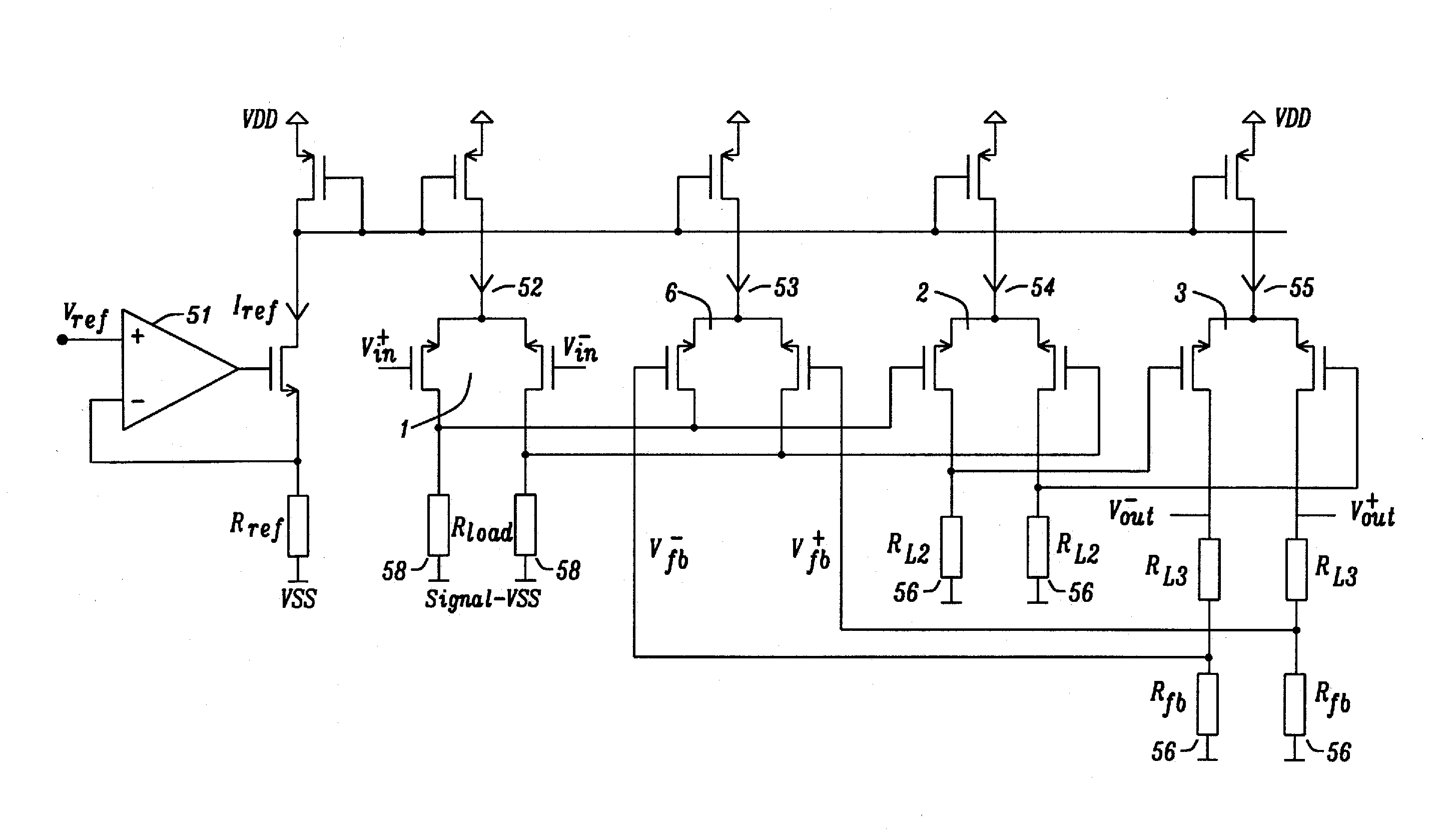
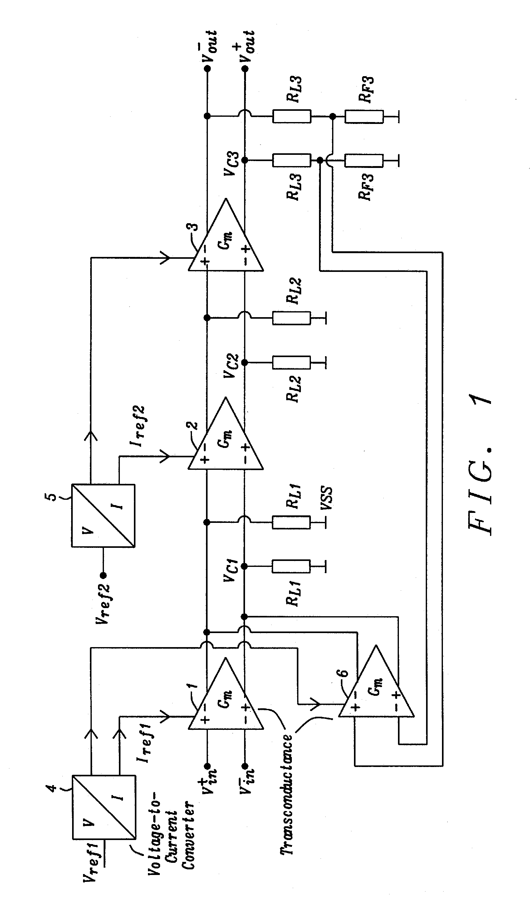
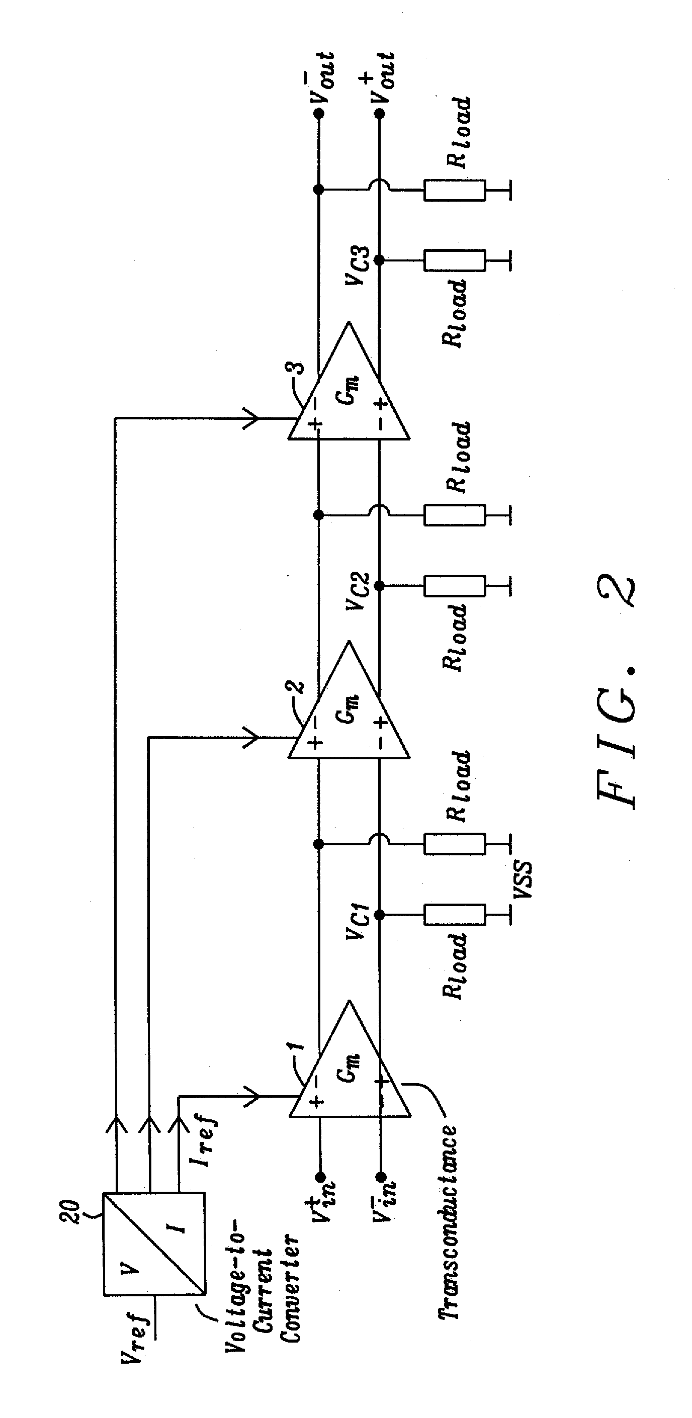
[0042]A preferred embodiment of the invention discloses an amplifier amplifying low frequency signals in the range of 0-500 Hz to minimize residual offset, non-linearity and gain errors. A prerequisite is a low transition frequency between 1 / f-noise and white noise. This can be achieved if only PMOS transistors are used in the amplifier circuit, as the PMOS transistors exhibit lower 1 / f-noise than NMOS transistors. In the preferred embodiment of the invention resistors are used as load impedances. Alternatively transistors operating as resistors, inductors, diodes, transistors operating as diodes, or MOS diodes could be used as load impedances. The problem of the low gain bandwidth product is circumvented using more than one gain stage, e.g. three gain stages. Therefore the amplifier disclosed has a very low noise density, namely below 30 nV...


PUM


Abstract

Disclosed are systems and methods to achieve a low noise, fully differential amplifier with controlled common mode voltages at each stage output but without the requirement of a common mode feedback loop. Common mode voltages are adjusted by adjusting the currents flowing through the load impedances (bias currents) wherein the currents are derived from one or more voltage-to-current converters based on an impedance that matches to the load impedances of the stages of the amplifier. The amplifier invented is primarily used for amplification of low frequency signals. The amplifier has one or more gain stages applying only one conduction type of transistors of an IC technology that has the lowest transition frequency between 1 / f noise and white noise to achieve a low chopping or autozeroing frequency.

Description

BACKGROUND OF THE INVENTION[0001](1) Field of the Invention[0002]This invention relates generally to amplifiers and relates more specifically to low-noise CMOS amplifiers primarily for amplification of low frequency signals.[0003](2) Description of the Prior Art[0004]Low noise amplifiers realized in CMOS technologies must suppress 1 / f-noise and DC-offset if low frequency signals need to be processed. 1 / f noise or Pink noise is a signal or process with a frequency spectrum such that the power spectral density is inversely proportional to the frequency, wherein white is the noise that has constant magnitude of power over frequency. The practice is the use of chopping or autozeroing (correlated double sampling of input offset) to eliminate the 1 / f noise. The achievable noise limit by use of autozeroing is about 10 to 15 dB above the white noise of the amplifier of the Autozero circuit. This is a result of undersampling of white band noise. Chopper amplifiers have a noise limit equal to...

Claims


Application Information

Patent Timeline
Patent Type & Authority Applications(United States)
IPC IPC(8): H03F3/45
CPCH03F3/45183H03F1/26
Inventor KILLAT, DIRK
Owner DIALOG SEMICONDUCTOR GMBH
Why Eureka
Try Eureka