Dual port SRAM having reduced cell size and rectangular shape

Active Publication Date: 2013-07-04
STMICROELECTRONICS INT NV
View PDF5 Cites 31 Cited by
  • Summary
  • Abstract
  • Description
  • Claims
  • Application Information

AI Technical Summary

Benefits of technology

[0021]This particular arrangement has a number of advantageous. First, the active areas of the storage nodes can each be designed to better perform its respective function for the transistor of which is a drain. Since each of the active areas for the storage transistors are physically isolated from each other and is the active area for just a single transistor and is not part of the pass gates, the shape, size and to some extent, the location of each, can be selected to permit the transistor of which it is a part to best perform its function in the memory cell, whether that of a pull-up transistor, a pass gate or a pull-down transistor. Each of these transistors has a specific and width to length ratio that will provide better performance for a given size. The size each active area can therefore be selected to provide a very small memory cell and the shape and location selected for high performance without having to be concerned about the trade off of the performance of another transistor that may share the same active area. Similarly, the active area for the pass gates is physically separate from the active area of both the pull-up an pull-down transistors so that its size and shape can be selected to better perform the function of a pass gate without having to be concerned with the performance tradeoffs of having to design the active area to also function as part of the storage node transistors.
[0022]In one embodiment, metal 1, called M1, is a blanket layer deposited over exposed conductive layers without the use of con

Problems solved by technology

In a memory cell layout of this type, the performance is degraded due to a high wordline capacitance which results in a high wordline RC time constant.
Other features of the layout of the memory cell create additional problems.
The result will be rounded edges and that the available width of the transistor is reduce resulting in degraded cell performance.
In addition, if a misalignment occurs, the gate electrode of the PG transistors may not be in the expected location unless the width is increased.
This will result in a greater mismatch between the pass gates and the other transistors, thus significantly degrading SRAM cell performance.
In addition, there will be problems in current grabbing at the intersection junction.
Therefore, some portions of PD-1 and PD-2 will have greater current densities than other portions and significant problems further degrading performance and impacting the reliability.
In addition, junction linkage is also a problem in a cell layout of this type.
The extended current path, and having to pass through repeated contacts,

Method used


Image

  • Dual port SRAM having reduced cell size and rectangular shape
  • Dual port SRAM having reduced cell size and rectangular shape
  • Dual port SRAM having reduced cell size and rectangular shape

Examples


Embodiment Construction

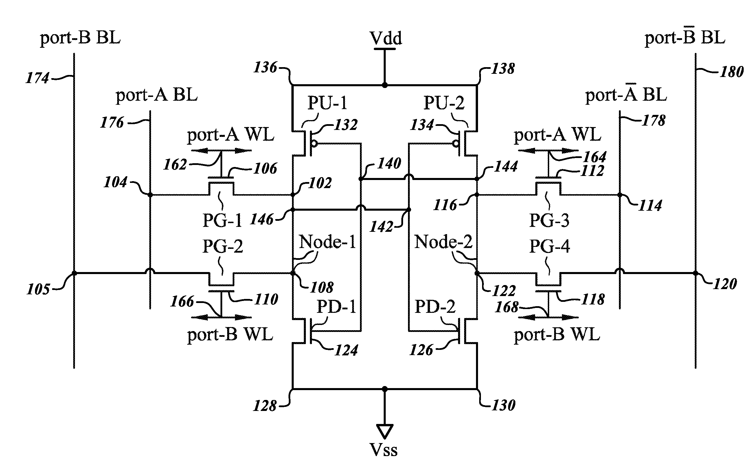
[0042]A new layout is provided for a dual port memory cell as illustrated in FIGS. 6-13, an alternative embodiment of which is shown in FIGS. 14 and 15.

[0043]The figures as shown herein are generally to scale with respect to the specific layouts. Namely, the features as shown in the layouts of FIGS. 7-15 are examples that represent the actual relative dimensions of the structures in one embodiment and show the feature sizes relative to each other. Some variation may exist between the different features as shown in these embodiments and their sizes relative to each other, and still fall within use of the present invention since the scope of the invention is defined by the claims and not by the figures or the specification. Namely, the location and general shape of the structures as shown herein constitutes a novel layout with advantageous and unexpected properties. A layout of the type shown herein may have many different sizes of components in different sizes relative to each other ...


PUM


Abstract

A dual port SRAM has two data storage nodes, a true data and complementary data. A first pull down transistor has an active are that forms the drain region of the first transistor and the true data storage node that is physically isolated from all other transistor active areas of the memory cell. A second pull down transistor has an active area that form the drain region of a second transistor that is the complementary data node that is physically isolated from all other transistor active areas of the memory cell.

Description

BACKGROUND[0001]1. Technical Field[0002]This invention relates to dual port SRAMs and, in particular, to a dual port SRAM having a reduced feature size in a rectangular-shaped cell layout.[0003]2. Description of the Related Art[0004]A dual port SRAM circuit is shown in FIG. 1 of a type well known in the art. Dual port SRAMs are particularly advantageous in certain types of memories to allow fast access for reading and writing. For example, dual port SRAMs may be used for the internal memory of a microprocessor in various stack registers. A dual port SRAMs is also frequently used in high speed communications, image processing, a FIFO and other circuits in which high speed and high reliability are required while accessing the memory cell through multiple ports during time periods which may overlap and even occur simultaneously. For these reasons, dual port SRAMs of the circuit type as shown in FIG. 1 have particular benefits across a wide range of products.[0005]Embedded SRAMs are par...

Claims


Application Information

Patent Timeline
IPC IPC(8): G11C5/06
CPCG11C11/412H01L27/1104H01L27/0207H10B10/12H10B10/00
Inventor KUMAR, SHISHIRDIPTI, DIBYAMALINGE, PIERRE
Owner STMICROELECTRONICS INT NV
Why Eureka
Try Eureka