Method for manufacturing photovoltaic cell

a photovoltaic cell and manufacturing technology, applied in the field of photovoltaic cell manufacturing, can solve the problems of photoelectric conversion performance deterioration and absorption loss, and achieve the effects of reducing resistance, efficiently preventing the deterioration of photoelectric conversion performance, and reducing the resistan

Inactive Publication Date: 2013-08-08
FUJI ELECTRIC CO LTD
View PDF6 Cites 1 Cited by
  • Summary
  • Abstract
  • Description
  • Claims
  • Application Information

AI Technical Summary

Benefits of technology

[0035]According to the invention, the following effects can be obtained.
[0036]The method for manufacturing a photovoltaic cell according to the invention relates to a method for manufacturing a photovoltaic cell including a structure in which a first electrode, a photoelectric conversion layer and a second electrode are laminated on one surface of a substrate in this order, and the photoelectric conversion layer is arranged as a multi-junction type photoelectric conversion layer in which a plurality of photoelectric conversion units are laminated while each of the photoelectric conversion units has a plurality of layers. The method for manufacturing the photovoltaic cell includes at least one step in which a surface of a layer formed in a process after the thickest one of the layers in the bottom one of the photoelectric conversion units formed on the first electrode is formed and before the thickest one of the layers in the top one of the photoelectric conversion units is formed is washed in the process.
[0037]Accordingly, a pin hole generated after a foreign substance is removed by the washing and in the layers that have been laminated till the washing can be buried with layers laminated after the washing. In addition, the layers with which the pin hole is buried include the thickest layer in the photoelectric conversion unit laminated next. It is therefore possible to efficiently preventing the deterioration of the photoelectric conversion performance caused by the adhesion of the foreign substance and the occurrence of leakage without remarkably lowering the resistance between the first electrode and the second electrode in the place where the pin hole is generated.
[0038]The method for manufacturing the photovoltaic cell according to the invention further includes the step of applying a reverse voltage between the first electrode and the second electrode after the second electrode is formed. Accordingly, a leak source can be removed due to the application of the reverse voltage so as to further efficiently prevent the deterioration of the photoelectric conversion performance caused by the adhesion of the foreign substance and the occurrence of leakage.
[0039]The method for manufacturing the photovoltaic cell according to the invention includes the step of applying hydrogen plasma treatment, argon plasma treatment or CF4 plasma treatment to the washed surface after the washing. Accordingly, the superficial layer of the washed surface degraded or contaminated by the washing is removed so that the surface can be well joined to a layer that is formed further thereon. It is therefore possible to improve the photoelectric conversion performance of the photovoltaic cell, with the result that it is possible to prevent the deterioration of the photoelectric conversion performance caused by the adhesion of the foreign substance.
[0040]In the method for manufacturing the photovoltaic cell according to the invention, film thickness of a layer to be washed is formed to be thicker than a designed film thickness in advance before the washing, and etching is performed by applying the hydrogen plasma treatment, the argon plasma treatment or the CF4 plasma treatment to the washed surface after the washing so as to make the film thickness of the washed layer as large as the predetermined designed film thickness. Accordingly, the film thickness of the washed layer can be prevented from being made thinner than the predetermined designed film thickness due to the washing.

Problems solved by technology

On the other hand, the p layer and the n layer do not have substantial contribution to the photoelectric conversion function, but the light absorbed by these layers causes an absorption loss.
When a foreign substance adheres to films that are being formed, there is a possibility that the photoelectric conversion performance may deteriorate due to the generation of a pin hole etc.

Method used


Image

  • Method for manufacturing photovoltaic cell
  • Method for manufacturing photovoltaic cell
  • Method for manufacturing photovoltaic cell

Examples


first embodiment

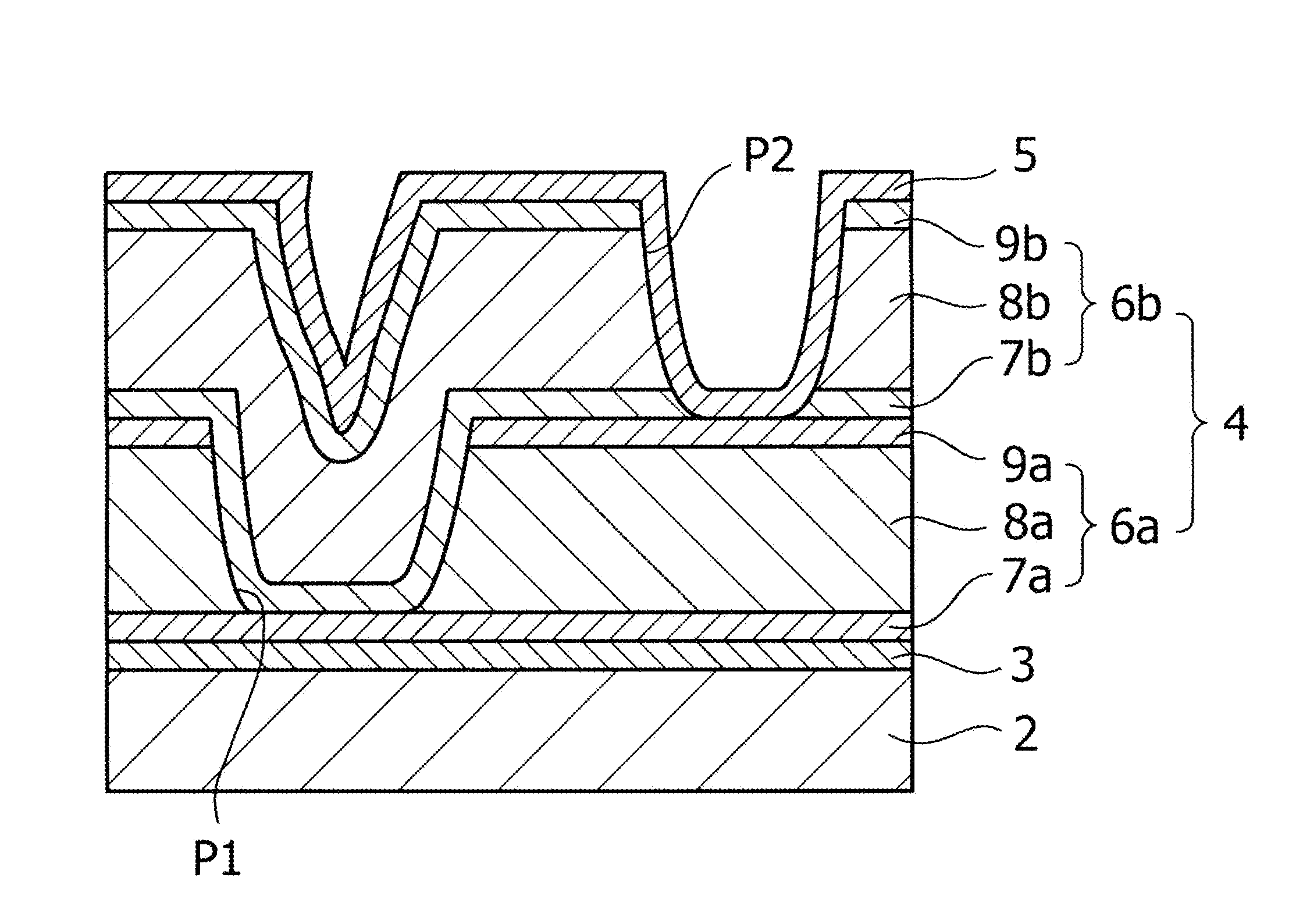
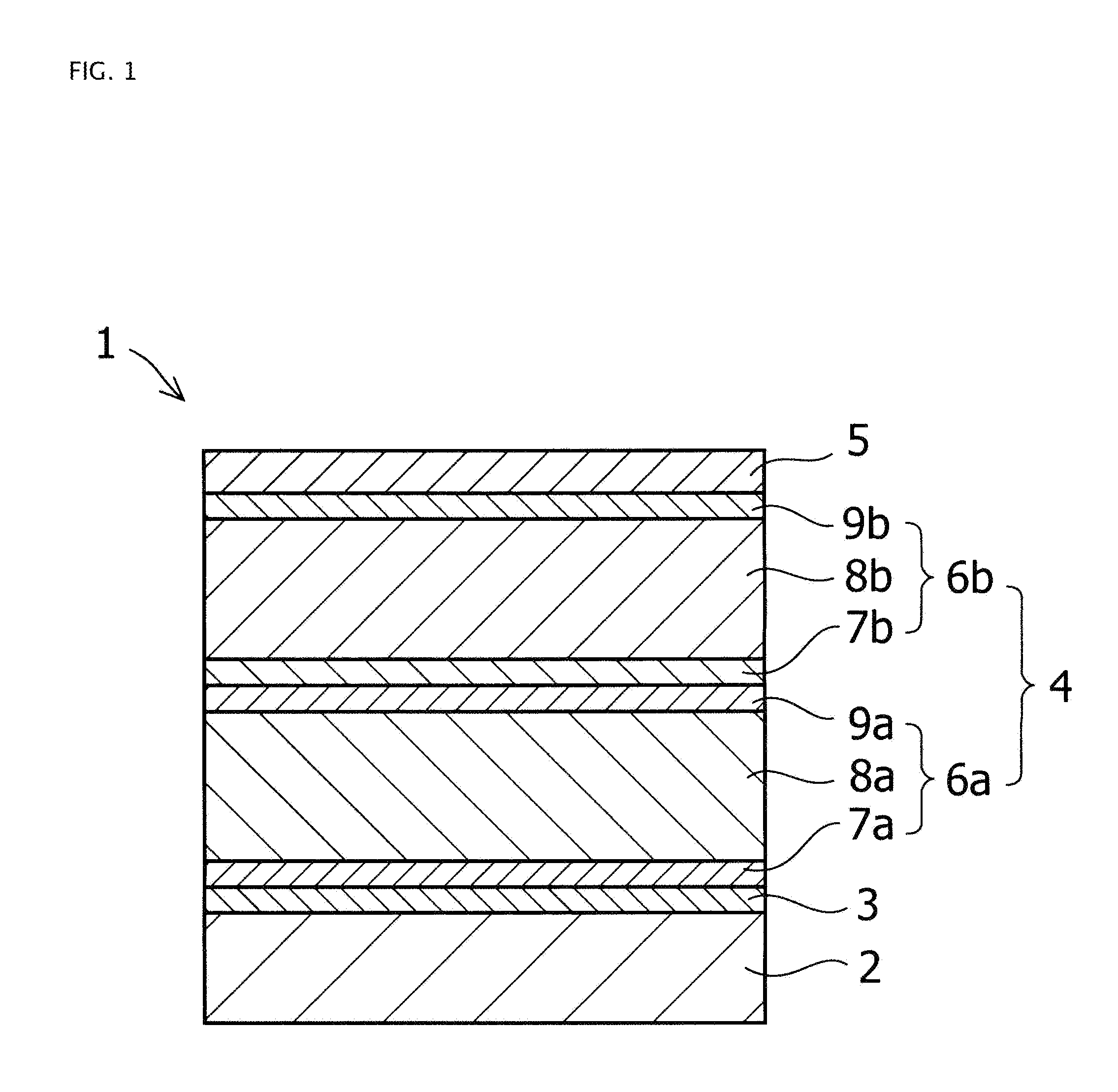
[0060]A method for manufacturing a photovoltaic cell in a first embodiment of the invention will be described below. As shown in FIG. 1, a photovoltaic cell 1 in the first embodiment of the invention has a laminate structure in which a first electrode 3, a photoelectric conversion layer 4 and a second electrode 5 are laminated on one surface of a substrate 2 in this order. An impermeable plastic substrate is used as the substrate 2, and the second electrode 5 side serves as the light receiving side. A heat-resistant plastic substrate such as a PI (polyimide) based film, a PEN (polyethylene naphthalate) based film, a PES (polyether sulfone) based film, a PET (polyethylene terephthalate) based film, an aramid based film, etc. may be used for an impermeable flexible substrate as the substrate 2. Moreover, a conductive substrate such as stainless steel foil, or a glass substrate or the like other than flexible substrates may be used as the substrate 2.

[0061]The first electrode 3 is arra...

second embodiment

[0078]A method for manufacturing a photovoltaic cell in a second embodiment of the invention will be described below. A fundamental form in the method for manufacturing a photovoltaic cell in the second embodiment is the same as that in the method for manufacturing a photovoltaic cell in the first embodiment. Elements similar to those in the first embodiment will be described using similar reference signs and names to those in the first embodiment. Here, description will be made on a different configuration from that of the first embodiment.

[0079]As shown in FIG. 4, a photovoltaic cell 20 in the second embodiment has a laminate structure in which a first electrode 3, a photoelectric conversion layer 21 and a second electrode 5 are laminated on one surface of a substrate 2 in this order.

[0080]The photoelectric conversion layer 21 has a first photoelectric conversion unit 22a laminated on the first electrode 3, a second photoelectric conversion unit 22b laminated on the first photoele...

third embodiment

[0088]A method for manufacturing a photovoltaic cell in a third embodiment of the invention will be described below. A fundamental form in the method for manufacturing a photovoltaic cell according to the third embodiment is the same as that in the method for manufacturing a photovoltaic cell in the first embodiment. Elements similar to those in the first embodiment will be described using similar reference signs and names to those in the first embodiment. Here, description will be made on a different configuration from that of the first embodiment.

[0089]As shown in FIG. 5, a photovoltaic cell 30 in the third embodiment has a laminate structure in which a first electrode 32, a photoelectric conversion layer 33 and a second electrode 34 are laminated on one surface of a substrate 31 in this order. An impermeable plastic substrate is used as the substrate 31, and the second electrode 34 side serves as the light receiving side. In addition, similar materials to those for the substrate ...


PUM


Abstract

Provided is a method for manufacturing a photovoltaic cell capable of efficiently preventing deterioration of photoelectric conversion performance caused by adhesion of a foreign substance and occurrence of leakage without lowering manufacturing efficiency. The method for manufacturing a photovoltaic cell having a structure in which a first electrode, a photoelectric conversion layer and a second electrode are laminated on one surface of a substrate in this order, and the photoelectric conversion layer is arranged as a multi-junction type photoelectric conversion layer in which a plurality of photoelectric conversion units are laminated while each photoelectric conversion unit has a plurality of layers, the method including at least one step in which a surface of a layer formed in a process after the thickest layer in a photoelectric conversion unit is formed and before the thickest layer in any one of photoelectric conversion units further laminated is formed is washed in the process.

Description

TECHNICAL FIELD[0001]The present invention relates to a method for manufacturing a photovoltaic cell having a laminate structure in which a first electrode, a photoelectric conversion layer and a second electrode are laminated on one surface of a substrate in this order.BACKGROUND ART[0002]Photovoltaic cells include Si (silicon) based thin-film photovoltaic cells, compound based photovoltaic cells using no Si, etc. Generally, in such a photovoltaic cell, a first electrode, a photoelectric conversion layer and a second electrode are laminated on a permeable or impermeable substrate in this order. When the substrate is permeable, sunlight can be incident on both the first electrode and the second electrode, and both the first electrode side and the second electrode side of the photovoltaic cell can be set as light receiving sides. On the other hand, when the substrate is impermeable, the second electrode side of the photovoltaic cell is set as a light receiving side. A transparent ele...

Claims


Application Information

Patent Timeline
Patent Type & Authority Applications(United States)
IPC IPC(8): H01L31/18
CPCH01L31/03921H01L31/03923H01L31/076H01L31/206Y02E10/548H01L31/18Y02E10/541Y02P70/50
Inventor SHIMOSAWA, MAKOTO
Owner FUJI ELECTRIC CO LTD
Why Eureka
Try Eureka