Device and method for measuring via hole of silicon wafer

a technology of silicon wafer and via hole, which is applied in the direction of optical radiation measurement, instruments, material analysis, etc., can solve the problems of difficult to confirm whether a formed via hole is successfully formed to have a desired predetermined depth and diameter, circuits may not be electrically connected, and limited line width that can be implemented, etc., to achieve rapid and accurate measurement of the depth and diameter of the via hole. , the effect of high precision

Active Publication Date: 2013-08-15
KOREA RES INST OF STANDARDS & SCI
View PDF2 Cites 6 Cited by
  • Summary
  • Abstract
  • Description
  • Claims
  • Application Information

AI Technical Summary

Benefits of technology

[0025]According to the means of the present invention as described above, it is possible to accurately measure the depth and the diameter of the via hole formed in the silicon wafer without damaging the wafer silicon.
[0026]It is also possible to measure the depth and the diameter of the via hole of the silicon wafer rapidly and with high precision.
[0027]With the device and the method for measuring a via hole according to an embodiment of the present invention, via hole measurement resolution is improved and a signal to noise ratio is improved by using a pulse having a short pulse width.
[0028]With the device and the method for measuring a via hole according to a preferred embodiment of the present invention, it is possible to accurately confirm whether the via hole is defective rapidly in a non-destructive manner. Accordingly, utilization in the 3D semiconductor packing process is excellent, the yield of a semiconductor package is improved, and influence of mechanical vibration on measurement quality is minimized.

Problems solved by technology

A fine line width has been implemented through exposure in order to implement a highly integrated semiconductor circuit, but the line width that can be implemented is limited due to a diffraction limit.
Accordingly, it is difficult to confirm whether a formed via hole is successfully formed to have a desired predetermined depth and diameter.
If the wafer chip is stacked on another wafer chip after grinding when the via holes are formed with different diameters or depths, some circuits may not be electrically connected and a product defect may be caused.
In the conventional optical measurement method, in the case of a measurement method using a confocal microscope, it is difficult to make accurate depth decision due to a great depth measurement error caused by diffuse reflection at a side surface of the via hole and a bottom surface, and in the case of a measurement method using a white-light scanning interferometer, it is difficult to accurately measure the depth of the via hole due to a light not reaching the bottom surface of the via hole by a high aspect ratio of a measurement specimen or due to a diffraction phenomenon occurring at a via hole entrance.
The method using a scanning electron microscope (SEM) has a drawback in that it damages a specimen, and accordingly cannot be used for total wafer inspection in a semiconductor packaging process.

Method used


Image

  • Device and method for measuring via hole of silicon wafer
  • Device and method for measuring via hole of silicon wafer
  • Device and method for measuring via hole of silicon wafer

Examples


Embodiment Construction

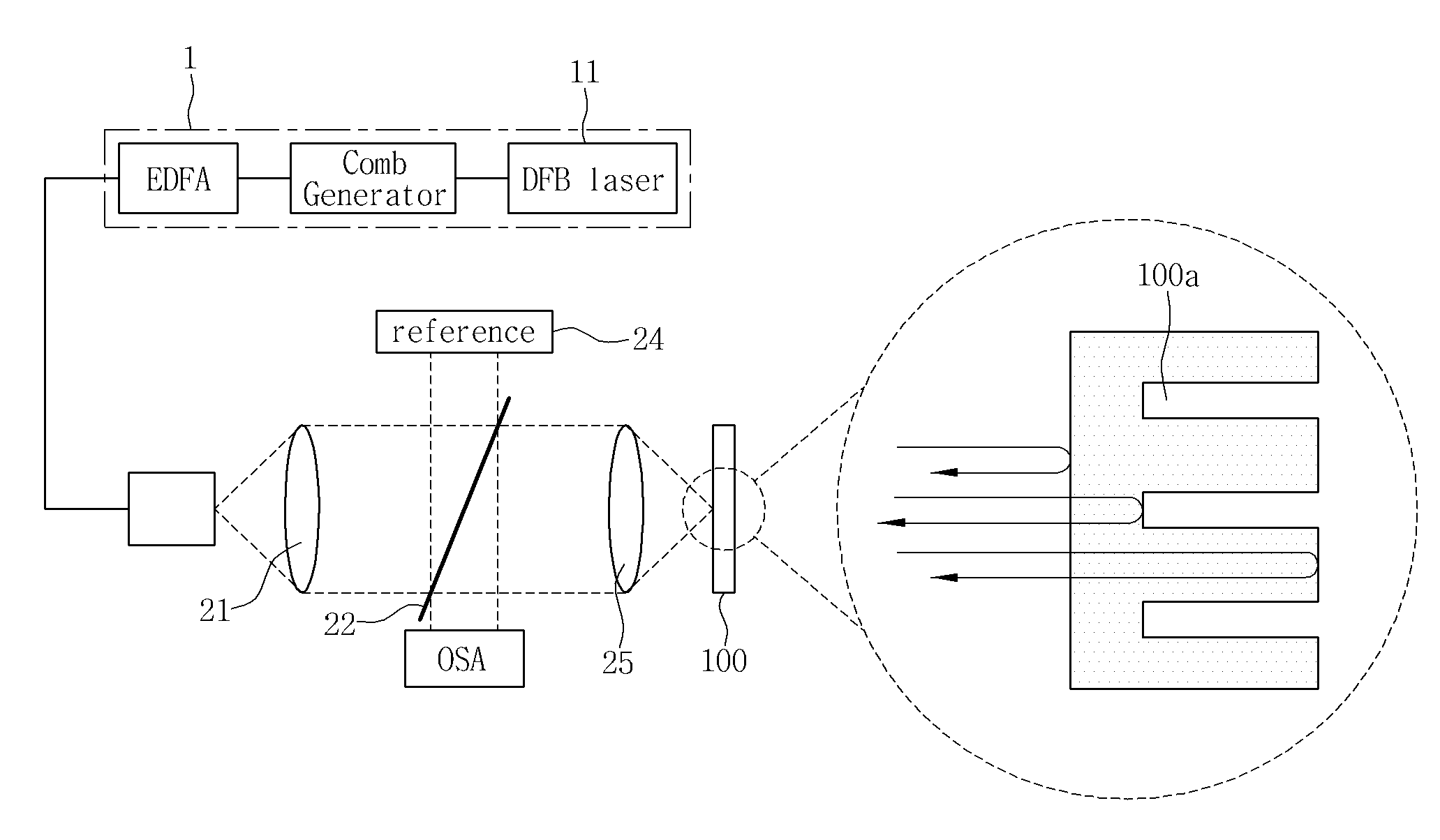
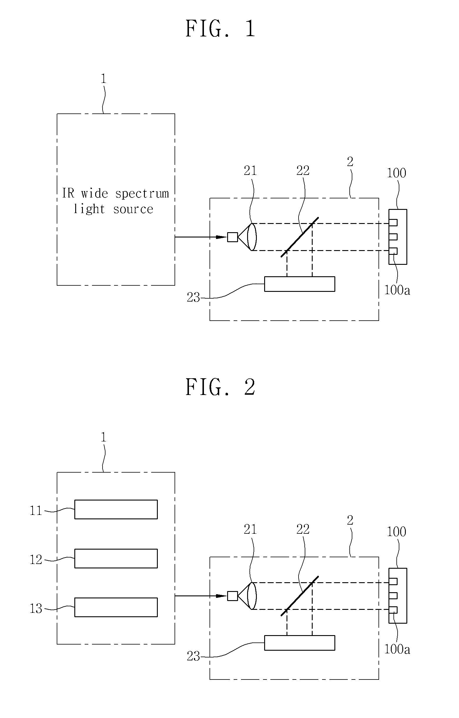
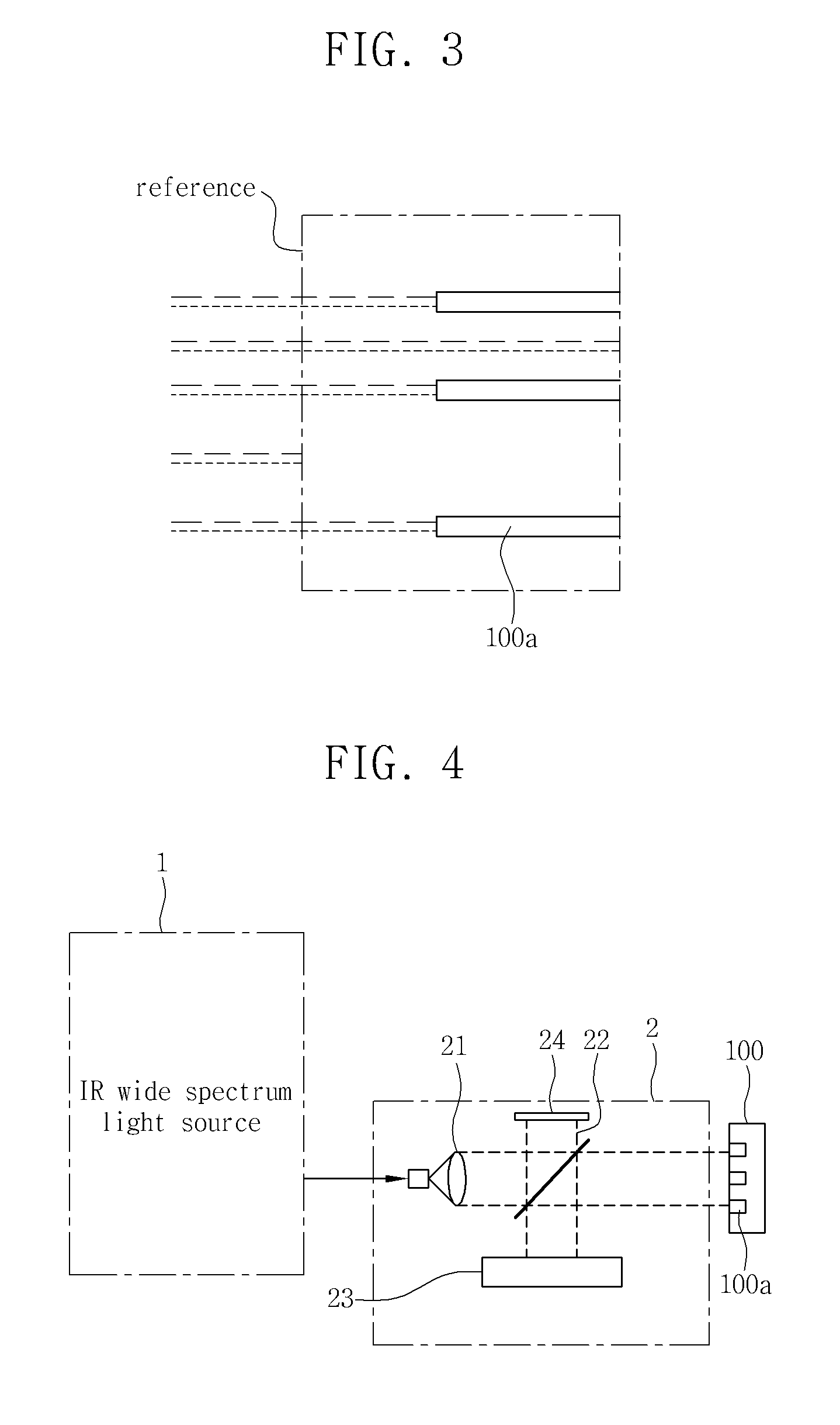
[0036]Hereinafter, a device for measuring a via hole of a silicon wafer according to the present invention will be described in detail with reference to the accompanying drawings.

[0037]A device for measuring a via hole of a silicon wafer according to an embodiment of the present invention is a device that measures a depth and a diameter of a via hole using an interference phenomenon of a light reflected by an interface of a bottom surface (hereinafter referred to as a bottom surface) of a via hole formed in a silicon wafer.

[0038]A semiconductor silicon wafer has a monocrystalline structure in which crystal is formed very uniformly. Accordingly, when light passes through a silicon wafer that is a single medium, the light is not refracted in the middle of the medium. Thus, it is possible to obtain information on a depth of the via hole from a light reflected by the interface of the bottom surface of the via hole and an outer interface of a front surface or a rear surface of the wafer....


PUM


Abstract

The present invention pertains to a device and a method for measuring a via hole of a silicon wafer, wherein it is possible to precisely measure the depth of the via hole without damaging the wafer. Broadband infrared light is radiated to a silicon wafer which has a superior light transmission property, so that the depth of the via hole may be measured from the light which is reflected from each boundary surface of the wafer and the interference signal of reference light. The via hole measuring device according to the present invention includes: a light source unit for generating broadband infrared light; and an interferometer for radiating the light generated from the light source unit to a silicon wafer, so as to measure the depth of a via hole formed on the wafer according to the spectrum period of the interference signal of the light, which is reflected from the silicon wafer.

Description

TECHNICAL FIELD[0001]The present invention relates to a device and a method for measuring a via hole, and more specifically, to a device and a method for measuring a via hole of a silicon wafer, which are capable of accurately measuring a depth and a diameter of a via hole without damaging the wafer.BACKGROUND ART[0002]A fine line width has been implemented through exposure in order to implement a highly integrated semiconductor circuit, but the line width that can be implemented is limited due to a diffraction limit.[0003]In order to overcome this, a method of reducing a diffraction limit using a light having a shorter wavelength than a visible light, such as extreme ultraviolet (EUV), and a 3D semiconductor packaging process of vertically stacking a number of wafer chips subjected to a process to increase an degree of integration have been proposed.[0004]In the 3D semiconductor packing process in which a number of wafer chips are vertically stacked, circuits of respective wafer la...

Claims


Application Information

Patent Timeline
Patent Type & Authority Applications(United States)
IPC IPC(8): G01B11/22G01B11/12
CPCG01B11/22G01B9/02008G01N2021/95653G01B11/12G01N21/9501G01B2210/56
Inventor JIN, JONG HANKIM, JAE WANKIM, JONG AHNKANG, CHU-SHIK
Owner KOREA RES INST OF STANDARDS & SCI
Why Eureka
Try Eureka