Semiconductor device, display device including semiconductor device, electronic device including semiconductor device, and method for manufacturing semiconductor device

Inactive Publication Date: 2013-08-15
SEMICON ENERGY LAB CO LTD
View PDF5 Cites 73 Cited by
  • Summary
  • Abstract
  • Description
  • Claims
  • Application Information

AI Technical Summary

Benefits of technology

[0027]A method for manufacturing a transistor with stable electric characteristics and little signal delay due to wiring resistance, used in a semiconductor device including an oxide semico

Problems solved by technology

Thus, there has been a problem in that the disclosed technique in Patent Document 1 is not a manufacturing me

Method used


Image

  • Semiconductor device, display device including semiconductor device, electronic device including semiconductor device, and method for manufacturing semiconductor device
  • Semiconductor device, display device including semiconductor device, electronic device including semiconductor device, and method for manufacturing semiconductor device
  • Semiconductor device, display device including semiconductor device, electronic device including semiconductor device, and method for manufacturing semiconductor device

Examples


embodiment 1

[0049]In this embodiment, one embodiment of a semiconductor device and a manufacturing method thereof will be described with reference to FIGS. 1A to 1C, FIGS. 2A to 2E, FIGS. 3A to 3D, FIGS. 4A to 4D, and FIGS. 5A to 5C. In this embodiment, a transistor using an oxide semiconductor film is described as an example of the semiconductor device.

[Structural Example 1 of Semiconductor Device]

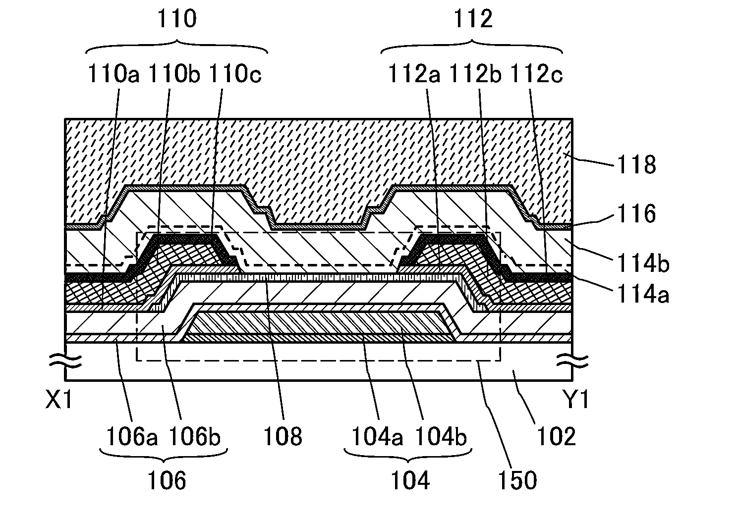
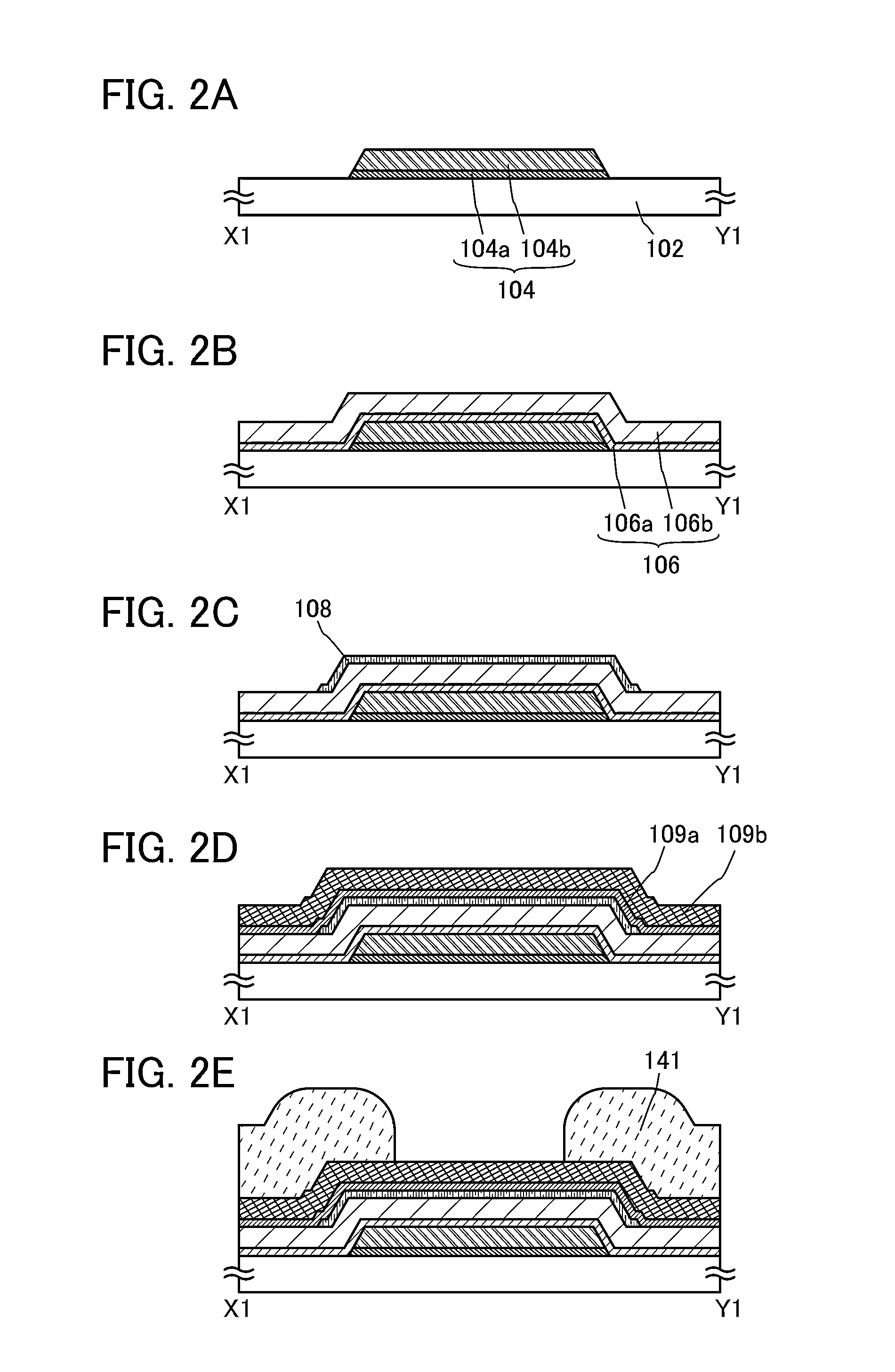
[0050]FIGS. 1A to 1C illustrate a structural example of a transistor 150. FIG. 1A is a plan view of the transistor 150, FIG. 1B is a cross-sectional view taken along the line X1-Y1 in FIG. 1A, and FIG. 1C is a cross-sectional view taken along the line V1-W1 in FIG. 1A. Note that in FIG. 1A, some components of the transistor 150 (e.g., a gate insulating film 106) are not illustrated for clarity.

[0051]The transistor 150 illustrated in FIGS. 1A to 1C includes a gate electrode 104 formed over a substrate 102, a gate insulating film 106 formed over the gate electrode 104, an oxide semiconductor film 108 f...

embodiment 2

[0180]In this embodiment, a modification example of the semiconductor device in Embodiment 1 and a method for manufacturing a semiconductor device, which is different from that in Embodiment 1, will be described with reference to FIGS. 6A and 6B, FIGS. 7A to 7D, and FIGS. 8A to 8D. Note that portions similar to those in FIGS. 1A to 1C, FIGS. 2A to 2E, FIGS. 3A to 3D, FIGS. 4A to 4D, and FIGS. 5A to 5C are denoted by the same reference numerals, and description thereof is omitted.

[Structural Example 2 of Semiconductor Device]

[0181]FIGS. 6A and 6B illustrate a structural example of a transistor 250 and a signal line region 260. FIG. 6A is a plan view of the transistor 250 and the signal line region 260. FIG. 6B is a cross-sectional view taken along the line X2-Y2 in FIG. 6A. Note that in FIG. 6A, some components of the transistor 250 and the signal line region 260 (e.g., a gate insulating film 206 and a second metal film 210b) are omitted to avoid complexity.

[0182]A semiconductor devi...

embodiment 3

[0220]A display device with a display function can be manufactured using the transistor exemplified in Embodiment 1 or Embodiment 2 and the signal line exemplified in Embodiment 2. Moreover, some or all of the driver circuits which include the transistor can be formed over a substrate where the pixel portion is formed, whereby a system-on-panel can be obtained. An example of the display device will be described with reference to FIG. 9.

[0221]In FIG. 9, a sealant 312 is provided so as to surround a pixel portion 302, a source driver circuit portion 304, and a gate driver circuit portion 306 which are provided over a first substrate 300. The second substrate 301 is provided over the pixel portion 302, the source driver circuit portion 304, and the gate driver circuit portion 306. Thus, the pixel portion 302, the source driver circuit portion 304, and the gate driver circuit portion 306 are sealed together with a display element by the first substrate 300, the sealant 312, and the seco...


PUM


Abstract

A method for manufacturing a transistor with stable electric characteristics and little signal delay due to wiring resistance, used in a semiconductor device including an oxide semiconductor film. A semiconductor device including the transistor is provided. A high-performance display device including the transistor is provided.

Description

BACKGROUND OF THE INVENTION[0001]1. Field of the Invention[0002]The present invention relates to semiconductor devices and methods for manufacturing the same. Further, the present invention relates to display devices and electronic devices having the semiconductor devices.[0003]2. Description of the Related Art[0004]Attention has been focused on a technique for forming a transistor using a semiconductor thin film formed over a substrate having an insulating surface (also referred to as thin film transistor (TFT)). The transistor is applied to a wide range of electronic devices such as an integrated circuit (IC) or an image display device (display device). A silicon-based semiconductor material is widely known as a material for a semiconductor thin film applicable to a transistor. As another material, an oxide semiconductor has been attracting attention.[0005]For example, a technique in which a transistor is manufactured using a Zn—O-based oxide or an In—Ga—Zn—O-based oxide as an oxi...

Claims


Application Information

Patent Timeline
IPC IPC(8): H01L29/786H01L29/66
CPCH01L29/78681H01L29/66742H01L29/7869H01L29/45H01L29/4908H01L29/66969H01L29/41733
Inventor YAMAZAKI, SHUNPEI
Owner SEMICON ENERGY LAB CO LTD
Why Eureka
Try Eureka