Low external resistance etsoi transistors

a technology of etsoi transistor and external resistance, which is applied in the direction of transistors, electrical devices, semiconductor devices, etc., can solve the problems of limiting the on-current, adversely affecting the performance of etsoi field effect transistors, and limited thickness of top semiconductor layers, so as to achieve the effect of low external resistan

Inactive Publication Date: 2013-08-22
IBM CORP
View PDF7 Cites 7 Cited by
  • Summary
  • Abstract
  • Description
  • Claims
  • Application Information

AI Technical Summary

Benefits of technology

[0003]A disposable dielectric structure is formed on a semiconductor-on-insulator (SOI) substrate such that all physically exposed surfaces of the disposable dielectric structure are dielectric surfaces. A semiconductor material is selectively deposited on semiconductor surfaces, while deposition of any semiconductor material on dielectric surfaces is suppressed. After formation of at least one gate spacer and source and drain regions, a planarization dielectric layer is deposited and planarized to physically expose a top surface of the disposable dielectric structure. The disposable dielectric structure is replaced with a replacement gate stack including a gate dielectric and a gate conductor portion. Lower external resistance can be provided without impacting the short channel performance of a field effect transistor device.

Problems solved by technology

However, high external resistance, i.e., high source / drain resistance, adversely impacts the performance of ETSOI field effect transistor by limiting the on-current.
This problem is caused by the limited thickness of a top semiconductor layer, as well as by dopant leaching from the extension regions into a buried oxide layer.

Method used


Image

  • Low external resistance etsoi transistors
  • Low external resistance etsoi transistors
  • Low external resistance etsoi transistors

Examples


Embodiment Construction

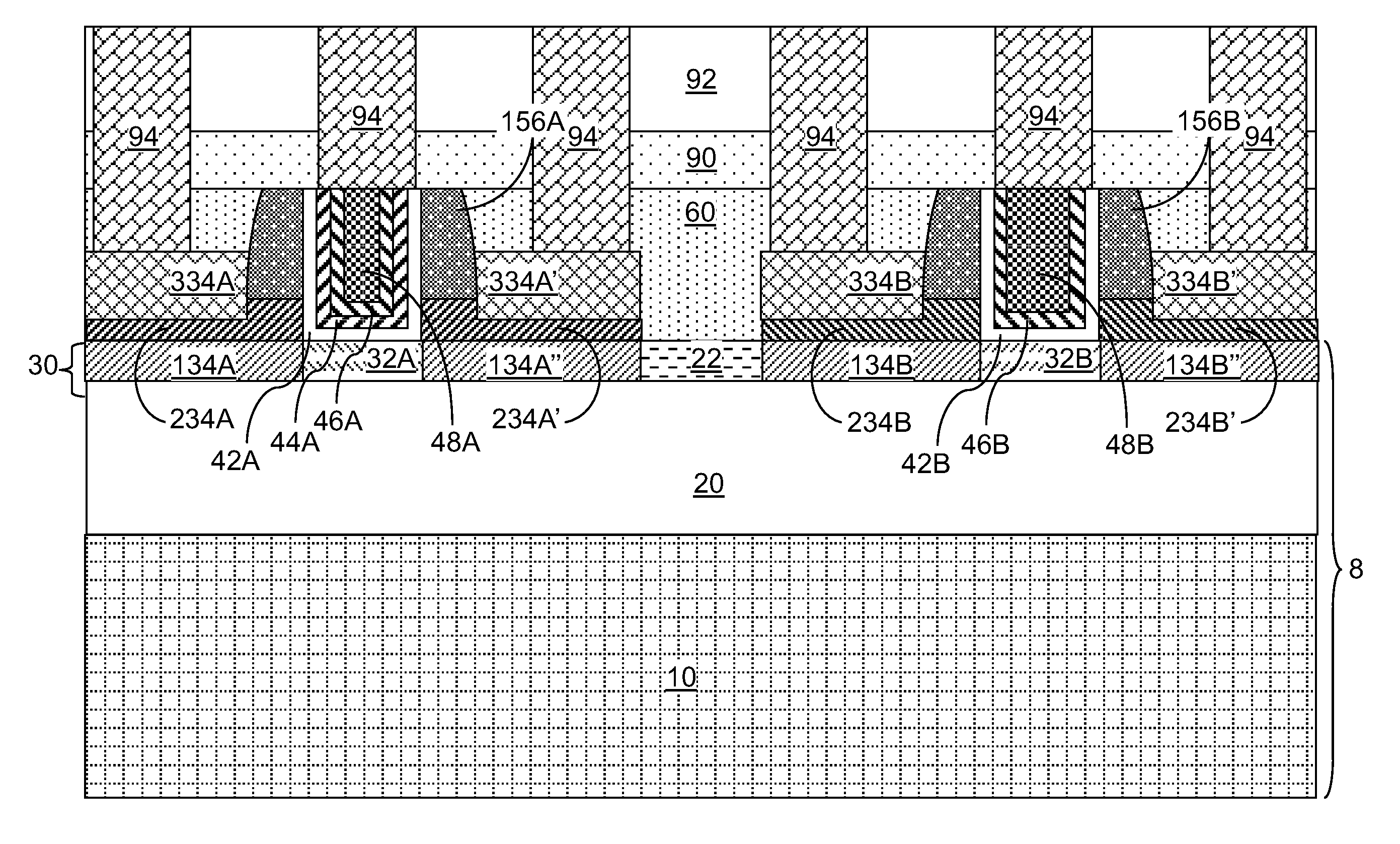
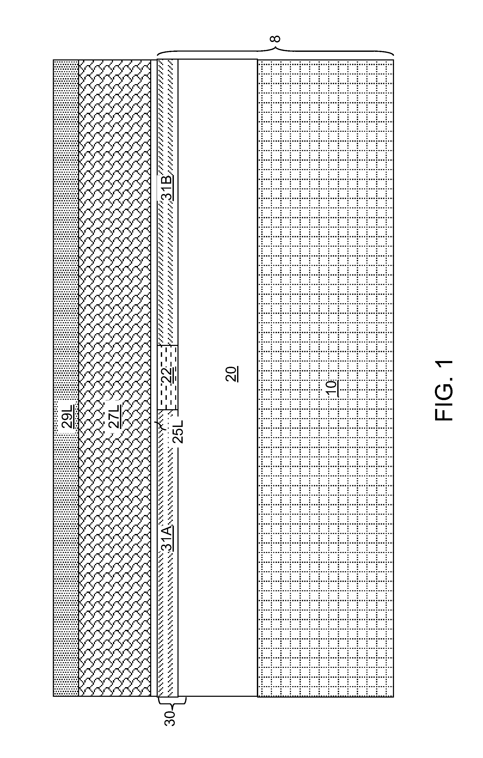
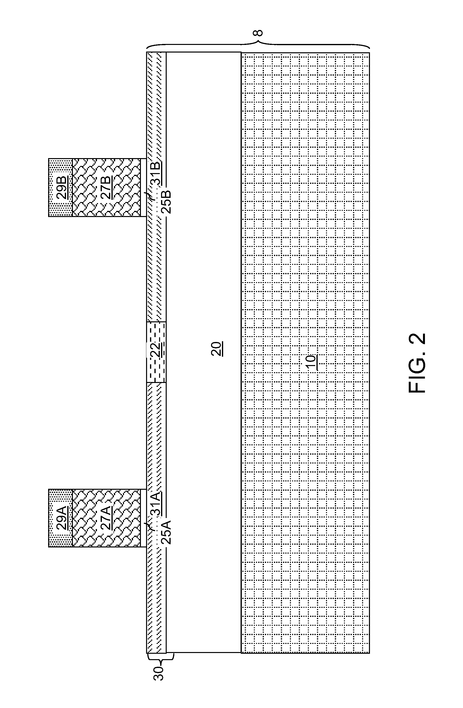
[0023]As stated above, the present disclosure relates to extremely thin semiconductor-on-insulator (ETSOI) field effect transistors having low external resistance, and methods of manufacturing the same, which are now described in detail with accompanying figures Like and corresponding elements mentioned herein and illustrated in the drawings are referred to by like reference numerals. The drawings are not necessarily drawn to scale.

[0024]Referring to FIG. 1, an exemplary semiconductor structure according to an embodiment of the present disclosure includes a semiconductor substrate 8. The semiconductor substrate 8 can be a semiconductor-on-insulator (SOI) substrate that includes a handle substrate 10, a buried insulator layer 20, and a top semiconductor layer 30. The handle substrate 10 provides mechanical support for the buried insulator layer 20 and the top semiconductor layer 30. The thickness of the handle substrate 10 can be, for example, from 50 microns to 2 mm, although lesser...


PUM


Abstract

A disposable dielectric structure is formed on a semiconductor-on-insulator (SOI) substrate such that all physically exposed surfaces of the disposable dielectric structure are dielectric surfaces. A semiconductor material is selectively deposited on semiconductor surfaces, while deposition of any semiconductor material on dielectric surfaces is suppressed. After formation of at least one gate spacer and source and drain regions, a planarization dielectric layer is deposited and planarized to physically expose a top surface of the disposable dielectric structure. The disposable dielectric structure is replaced with a replacement gate stack including a gate dielectric and a gate conductor portion. Lower external resistance can be provided without impacting the short channel performance of a field effect transistor device.

Description

BACKGROUND[0001]The present disclosure relates to semiconductor structures, and particularly to extremely thin semiconductor-on-insulator (ETSOI) field effect transistors having low external resistance, and methods of manufacturing the same.[0002]Extremely thin semiconductor-on-insulator (ETSOI) devices have been proposed to enable continued scaling of complementary metal-oxide-semiconductor (CMOS) devices with superior short channel characteristics at sub-20 nm gate lengths so that enhanced gate control can be provided to a thin semiconductor channel having a thickness not greater than 30 nm. However, high external resistance, i.e., high source / drain resistance, adversely impacts the performance of ETSOI field effect transistor by limiting the on-current. This problem is caused by the limited thickness of a top semiconductor layer, as well as by dopant leaching from the extension regions into a buried oxide layer. In order to enhance the performance of ETSOI field effect transistor...

Claims


Application Information

Patent Timeline
Patent Type & Authority Applications(United States)
IPC IPC(8): H01L29/786H01L21/336
CPCH01L21/823814H01L21/823842H01L29/4908H01L29/42384H01L27/1203
Inventor JAGANNATHAN, HEMANTHKANAKASABAPATHY, SIVANANDA K.
Owner IBM CORP
Why Eureka
Try Eureka