Method and Apparatus for Plasma Dicing a Semi-conductor Wafer

a technology of semi-conductor wafers and plasma dicing, which is applied in the direction of semiconductor devices, thin material processing, electric discharge tubes, etc., can solve the problems of reducing the number of good dies produced, affecting the cost effectiveness of this approach, and limitations of the dicing techniqu

Active Publication Date: 2013-09-05
PLASMA THERM
View PDF2 Cites 31 Cited by
  • Summary
  • Abstract
  • Description
  • Claims
  • Application Information

AI Technical Summary

Benefits of technology

[0027]The present invention describes a plasma processing apparatus which allows for plasma dicing of a semiconductor substrate. After device fabrication and wafer thinning, the front side (circuit side) of the substrate is masked using conventional masking techniques which protects the circuit components and leaves unprotected areas between the die. The substrate is mounted on a thin tape which is supported within a rigid frame. The substrate / tape / frame assembly is transferred into a vacuum processing chamber and exposed to reactive gas plasma where the unprotected areas between the die are etched away. During this process, the frame and tape are protected from damage by the reactive gas plasma. The processing leaves the die completely separated. After etching, the substrate / tape / frame assembly is additionally exposed to plasma which removes potentially damaging residues from the substrate surface. After transfer of the substrate / tape / frame assembly out of the process chamber, the die are removed from the tape using well known techniques and are then further processed (e.g., packaged) as necessary.

Problems solved by technology

A mechanical clamping mechanism, in which a downward force is applied to the top side of the substrate, may be used, though this may cause contamination due to the contact between the clamp and the substrate.
Such mechanical wafer dicing techniques have limitations which affect the cost effectiveness of this approach.
Chipping and breakage along the die edges can reduce the number of good die produced, and becomes more problematic as wafer thicknesses decrease.
Mechanical means are also limited to separation along straight lines and the production of square or oblong shaped chips.
This may not represent the underlying device topology (e.g., a high power diode is round) and so the rectilinear die format results in significant loss of useable substrate area.
Laser dicing also has limitations by leaving residual material on the die surface or inducing stress into the die.
Most tools used for wafer dicing (saws or laser based tools) are designed to handle substrates in this configuration and a number of standard fixtures have been established; however, such fixtures are very different from the substrates which they support.
Though such fixtures are optimized for use in current wafer dicing equipment, they cannot be processed in equipment which has been designed to process standard substrates.
Thus, current automated plasma etching equipment is not suitable for processing substrates fixtured for dicing and it is difficult to realize the benefits that plasma etch techniques should have for die separation.
While this technique allows standard plasma equipment to dice the wafer, the proposed technique will not be compatible with standard equipment downstream of the dicing operation.
In contrast to standard dicing techniques which singulate the substrate from the front side, this technique introduces additional complex and expensive steps which may negate some of the advantages of plasma dicing.

Method used


Image

  • Method and Apparatus for Plasma Dicing a Semi-conductor Wafer
  • Method and Apparatus for Plasma Dicing a Semi-conductor Wafer
  • Method and Apparatus for Plasma Dicing a Semi-conductor Wafer

Examples


Embodiment Construction

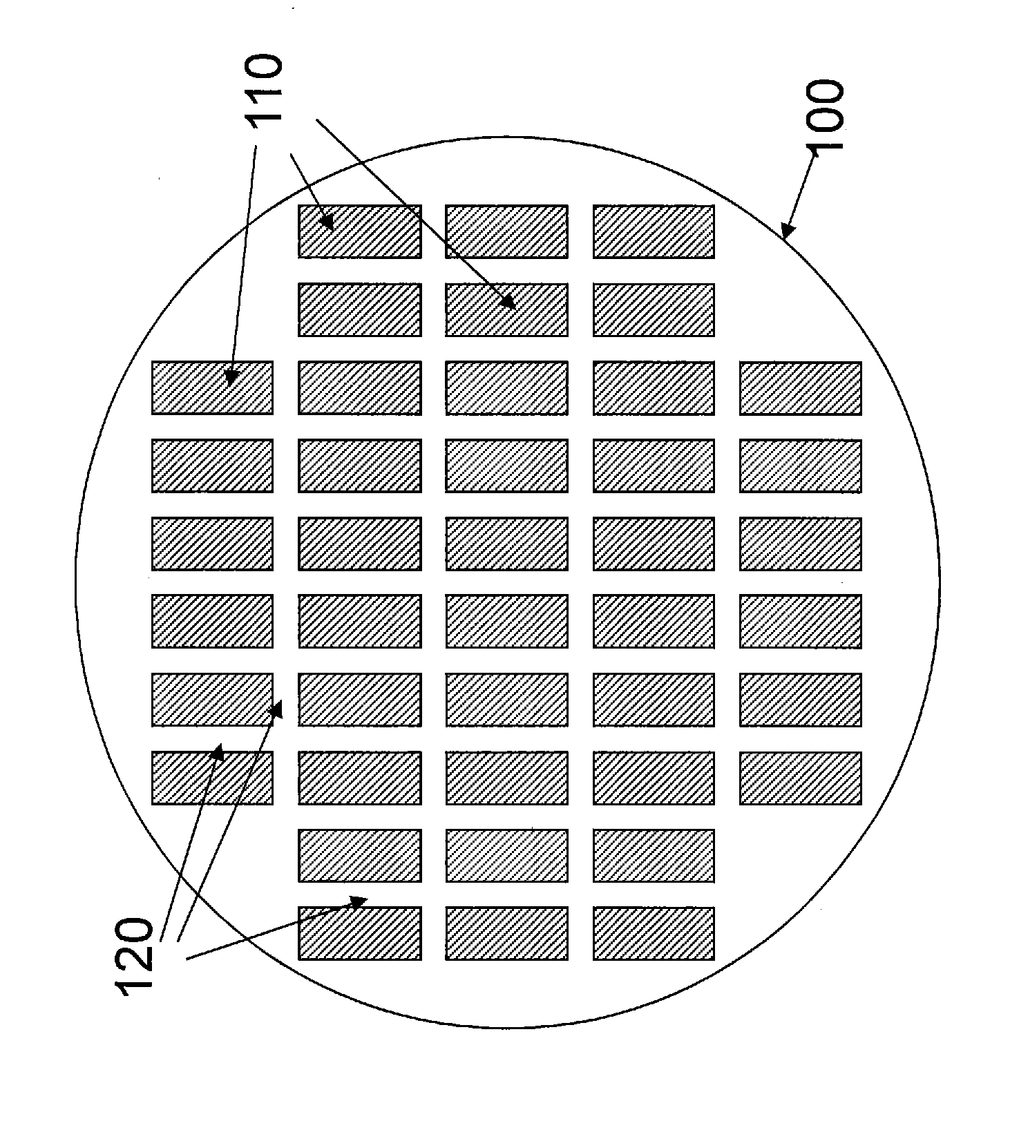
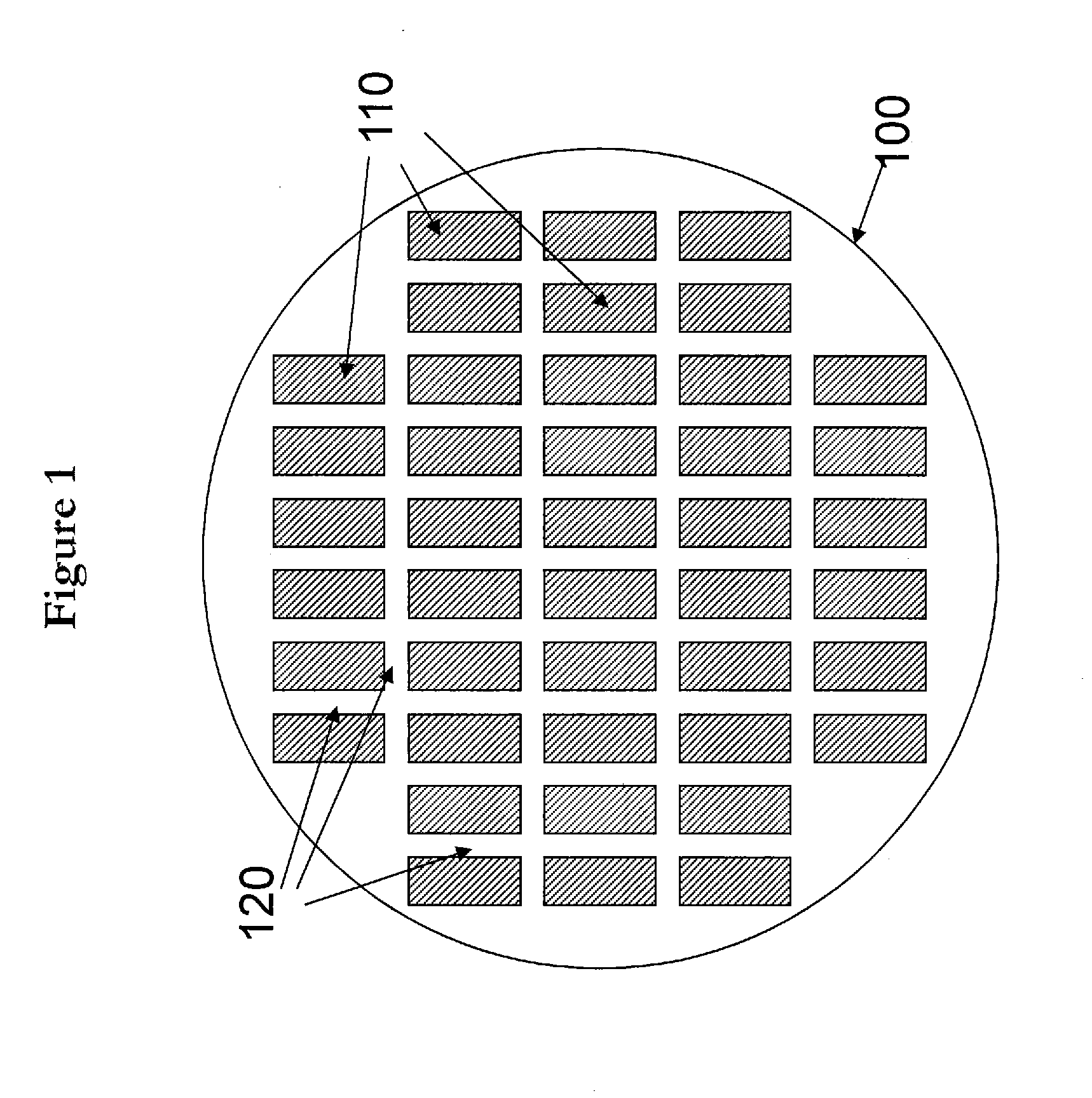
[0074]A typical semiconductor substrate after device fabrication is illustrated in FIG. 1. The substrate (100) has on its surface a number of areas containing device structures (110) separated by street areas (120) which allows for separation of the device structures into individual die. Although silicon is commonly used as a substrate material, other materials chosen for their particular characteristics are frequently employed. Such substrate materials include Gallium Arsenide and other III-V materials or non-semi-conductor substrates on which a semi-conducting layer has been deposited. Further substrate types may also include Silicon-On-Insulator (SOI) wafers and semiconductor wafers mounted on carriers. While the example above describes die separated by streets, aspects of the invention may be beneficially applied to other pattern configurations on a substrate.

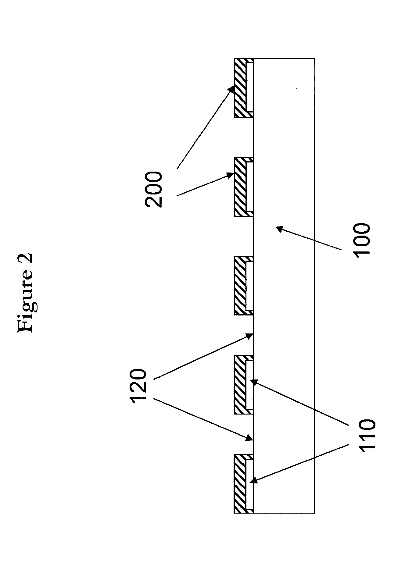
[0075]In the present invention, as is shown in a cross sectional view in FIG. 2, the device structures (110) are then cov...


PUM


Abstract

The present invention provides a method for plasma processing a substrate. The method comprising providing a process chamber having a wall; providing a plasma source adjacent to the wall of the process chamber; providing a work piece support within the process chamber; loading a work piece onto the work piece support, the work piece having a support film, a frame and the substrate; providing a cover ring above the work piece, the cover ring having at least one perforated region, and at least one non-perforated region; generating a plasma using the plasma source; and processing the work piece using the generated plasma.

Description

CROSS REFERENCES TO RELATED APPLICATIONS[0001]This application claims priority from and is related to commonly owned U.S. Provisional Patent Application Ser. No. 61 / 452,450 filed Mar. 14, 2011, entitled: Apparatus for Plasma Dicing a Semi-conductor Wafer, this Provisional Patent Application incorporated by reference herein. This application is a continuation-in-part of co-pending patent application Ser. No. 13 / 412,119 filed on Mar. 5, 2012, entitled: Method and Apparatus for Plasma Dicing a Semi-conductor Wafer, the contents of which are incorporated herein.FIELD OF THE INVENTION[0002]The invention relates to the use of an apparatus for the formation of individual device chips from a semi-conductor wafer, and in particular to an apparatus which uses plasma etching to separate the wafer into individual die.BACKGROUND[0003]Semiconductor devices are fabricated on substrates which are in the form of thin wafers. Silicon is commonly used as the substrate material, but other materials, su...

Claims


Application Information

Patent Timeline
Patent Type & Authority Applications(United States)
IPC IPC(8): H01L21/78
CPCY10S414/139H01J37/32495H01J37/32623H01J37/32651H01L21/3065H01L21/30655H01L21/31116H01L21/67011H01L21/67069H01L21/67739H01L21/6831H01L21/68735H01L21/68742H01L21/78H01L21/782H01L2221/68327H01J37/32155H01J37/32449H01J37/32422
Inventor GEERPURAM, DWARAKANATHPAYS-VOLARD, DAVIDMARTINEZ, LINNELLJOHNSON, CHRISJOHNSON, DAVIDWESTERMAN, RUSSELL
Owner PLASMA THERM
Why Eureka
Try Eureka