Physical contact layer for body-worn leadware using selective deposition

a physical contact layer and leadware technology, applied in the field of flexible electronics, can solve the problems of irritating, scratching, chafing, etc., designed to be comfortable for users, and complicating instances, so as to save material cost, avoid scrapping unused parts, and save material cost

Active Publication Date: 2013-09-26
MOLEX INC
View PDF7 Cites 30 Cited by
  • Summary
  • Abstract
  • Description
  • Claims
  • Application Information

AI Technical Summary

Benefits of technology

[0016]In another feature and advantage of embodiments of the invention, a puff ink comfort layer is selectively deposited only where it is desired and exactly where it is desired, by, for example, printing, spray coating, screen printing or coating, coating through a patterned or otherwise previously prepare mask, or other techniques. When compared to comfort layer production of the prior art, material cost is saved. The waste incurred in cutting a larger than required sheet of material and scrapping the unused part is avoided. On the contrary, the comfort layer is deposited in the precise amount and in the precise location as is desired in the final printed flexible electronics, with due allowance for manufacturing tolerance. Thus, material cost is saved compared to comfort layer production of the prior art.
[0017]In another feature and advantage of embodiments of the invention, a puff ink (or other) comfort layer can comprise certain dielectric properties. In embodiments, material and production costs can therefore be additionally reduced by using the puff ink comfort layer as a replacement for certain traditional dielectric layers, when compared to flexible printed electronics of the prior art. In embodiments, material costs are saved due to the dual role of the single comfort layer in embodiments of a particular application of a printed circuit; the separate dielectric layer materials are no longer required to be printed into the circuit. Production costs are likewise saved due to the dual role; the dielectric layer is now superfluous and no longer needs to be printed into the circuit. In embodiments where a dielectric layer is used with a puff ink comfort layer, embodiments of the puff ink comfort layer add to the insulation properties of the overall circuit.
[0018]In another feature and advantage of embodiments of the invention, a puff ink comfort layer comprises a waterproof barrier. In other embodiments, a puff ink comfort layer can be deposited on a heavy waterproofing layer to create a waterproof barrier that is still a soft and comfortable interface to the skin. As a result, the flexible printed electronics of embodiments can be used in water-laden environments. For example, embodiments of body-worn leads can be utilized in diagnostic or therapeutic devices worn in swimming pool testing or scuba diving applications. Additionally, in dry environments where liquid has a chance of contacting the printed electronics, embodiments of the flexible printed electronics are further protected from water damage by the waterproof barrier provided by embodiments of the comfort layer.
[0019]In another feature and advantage of embodiments of the invention, no memory fold is retained in the electronics after crimping or bending. As a result, body-worn leads are more easily affixed to a patient, and are more likely to remain affixed than the body-worn leads of the prior art. Additionally, the underlying electronics are not stressed or damaged by any permanent memory of a fold retained by the comfort layer, and measurement characteristics are more likely to be measured accurately than the body-worn leads of the prior art.
[0020]Because no memory fold exists in embodiments, myriad options for packaging embodiments of the printed flexible electronics are available. For example, embodiments can be rolled up or folded. As a result, the formatting of the packaging can be made to suit widely accepted and broadly used packaging, handling, and distribution methods, including those traditionally recognized in a medical environment. As a result, packaging and handling costs are reduced as no intermediary card insert is required, compared to packaging in the prior art. And further, the body-worn leads comprising embodiments of the printed flexible electronics allow handing in packaging more familiar and convenient to medical professionals and other end users.
[0021]Embodiments of the present application are not limited to medical applications. On the contrary, embodiments can be utilized, for example, in the context of “smart clothes” having electronics embedded within a piece of clothing for novelty or utility, or wearable computers, or any other application where electronics worn against the body necessitate a comfort layer between the electronic components and the wearer. For example, performance monitoring for humans and animals in stressful (combat or emergency) or competitive (sports) situations can also call for distributed sensing and collection of data. In addition, the expanded use of personal electronic devices for information and entertainment purposes will benefit from clothing attached leadware made more convenient with an efficiently generated comfort layer. More generally, the integration of electronic functionality with other uses of textiles, such as hospital gowns, blankets, tents, mattress covers, or pillow covers, for example, all benefit from the use of an economically constructed comfort layer to protect the user.

Problems solved by technology

As a result, intricate electrical circuits that are printed on flexible substrates can comprise printed flexible electronics.
However, this lead wire harness can further complicate instances where individual leads need to be broken out to make particular connections to individual sensing points.
However, because body-worn leadware is in contact with the patient's skin, it can be uncomfortable for the wearer or can cause irritation, chafing, or scratching of the wearer's skin.
The substrates, conductive layers, and dielectric layers that comprise traditional leads contain components with various organic or inorganic materials that are designed for a conductive, insulating, or semi-conductive purpose and are not necessarily designed to be comfortable to the user.
Indeed they have a stiffness and sharpness of edge which, just as with paper, can lead to cuts and abrasions.
However, traditional comfort layers suffer from problems in manufacturing, distribution, and use.
Further, there is often considerable waste of the comfort layer material because the traditional comfort layer manufacturing process typically starts with a whole web or sheet (100% coverage) of material which is die cut before lamination, and then die cut along with the final printed circuit when the assembly is singulated.
This is done because the various intricately-aligned features of the printed electronics can be difficult to align with the corresponding features in a pre-cut piece of comfort layer material.
Therefore, not only are additional steps incurred, thus increasing production cost, but comfort layer material is applied, then cut away and discarded during production, thus further increasing material costs.
Additionally, the packaging of traditional printed flexible electronics incorporating a comfort layer is problematic.
As a result, bending during the packaging impresses a “kink” which the part retains throughout its useful life.
These memory folds can be problematic during use of the leadware.
It can make the leads difficult to affix (and remain affixed) to the patient.
Memory folds can also lead to more interference between the leadware and items in the vicinity such as clothing, bedding, etc.
Likewise, there may be interference with the measurement of the patient's clinical information.
When compared to comfort layer production of the prior art, material cost is saved.
Thus, material cost is saved compared to comfort layer production of the prior art.

Method used


Image

  • Physical contact layer for body-worn leadware using selective deposition
  • Physical contact layer for body-worn leadware using selective deposition
  • Physical contact layer for body-worn leadware using selective deposition

Examples


Embodiment Construction

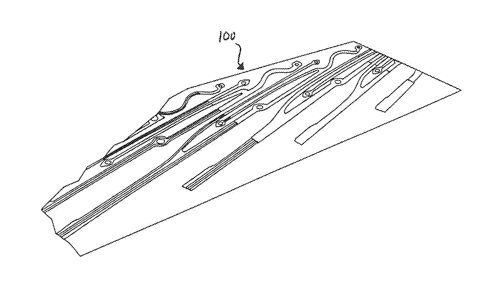
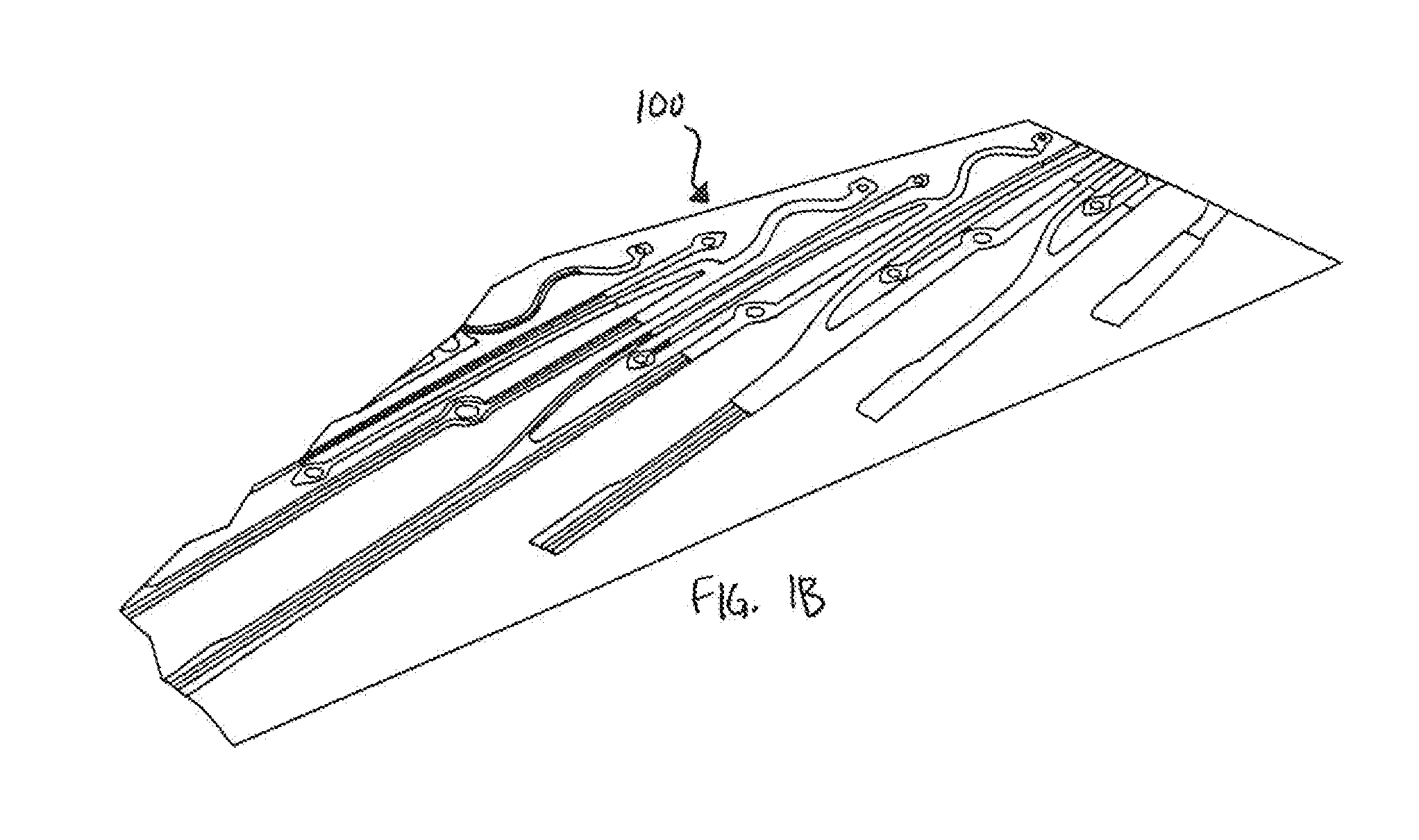
[0034]Referring generally to FIGS. 1B, 2 and 3A-3C, a set of flexible printed electronics 100 according to an embodiment are depicted. The set of flexible printed electronics 100 generally comprise individual circuit traces each having a substrate 102, a conductive layer 104, a dielectric layer 106, and a comfort layer 108. Of course, any particular embodiment can comprise greater or fewer layers, as the below-described embodiments are for illustration purposes only and are in no way limiting.

[0035]Substrate 102 comprises the base material onto which the conductive, non-conductive, and comfort components will be printed. Substrate 102 can be any suitable substrate in a sheet, roll, web, or similar structure. In an embodiment, substrate 102 comprises a fabric layer, such as cotton or polyester, woven, or non-woven. In other embodiments, substrate 102 comprises other flexible substrates such as polymer film such as polyethylene terephthalate film (PET), Polyethylene naphthalate (PEN),...


PUM

PropertyMeasurementUnit
conductiveaaaaaaaaaa
softaaaaaaaaaa
non-abrasive propertiesaaaaaaaaaa

Abstract

A printed electrical circuit and methods for additively printing electrical circuits. Patterned layers of conductive, insulating, semi-conductive materials, and other materials are print deposited on a flexible or rigid substrate to form electrical circuits. A buffering layer is selectively deposited to cover or encapsulate these materials to comprise a comfort layer that provides a soft and comfortable interface to the skin of a wearer. The comfort layer can be selectively deposited on the same press that the conductive, insulating, semi-conductive materials, and other materials are deposited. Further, the comfort layer is selectively deposited only where it is desired and exactly where it is desired.

Description

RELATED APPLICATION[0001]The present application claims the benefit of U.S. Provisional Application No. 61 / 613,067 filed Mar. 20, 2012, which is incorporated herein in its entirety by reference.TECHNICAL FIELD[0002]The invention relates generally to flexible electronics, and more particularly, to protective layers for printed flexible electronics, such as those used in body-worn leadware.BACKGROUND[0003]Flexographic, lithographic, gravure, screen printing, digital printing such as inkjet or drop on demand, and other processes, including those in which a central impression cylinder is used, are known in the art for printing a wide variety of articles. Recently, these and other processes and techniques have been used to print functional materials, including those required to make electrical circuits. Whereas etching and other subtractive processes for creating circuits are wasteful, relatively costly, and time-consuming, thereby limiting applicability and use, printing processes, by v...

Claims


Application Information

Patent Timeline
Patent Type & Authority Applications(United States)
IPC IPC(8): H05K1/02
CPCA61B5/04085A61B5/6805A61N1/0484Y10T156/10A61B2562/164H05K1/02A61B2562/125H05K1/038H05K1/0393A61B5/282A61B5/6804A61B5/6892A61B2562/166H05K1/0373H05K1/09H05K3/12H05K2201/05H05K2203/1333H05K2203/1366
Inventor SIME, DAVID G.KOBLE, RICHARD
Owner MOLEX INC
Why Eureka
Try Eureka