Method of forming a wiring pattern

a wiring pattern and wire pattern technology, applied in the direction of resistive material coating, liquid/solution decomposition chemical coating, superimposed coating process, etc., can solve the problems of increased manufacturing cost, inappropriate use, difficult control of process, etc., and achieve the effect of alleviating the difficulty of etching the finer wiring patterns from copper foil

Inactive Publication Date: 2013-09-26
HO CHIEN HAN +1
View PDF5 Cites 5 Cited by
  • Summary
  • Abstract
  • Description
  • Claims
  • Application Information

AI Technical Summary

Benefits of technology

[0009]In the method of the present invention, a wiring pattern is formed by using a screen printing method, but not by using an etching method. Consequently, there are no high cost and etching contamination issues. Furthermore, the difficulty in etching the finer wiring patterns from the copper foil can be alleviated.

Problems solved by technology

However, the current legislations for environment protection require that the highly contaminant byproducts formed during the etching process have to be recycled and properly treated, which increases the manufacture cost.
Because the chemical etching process is difficult to be controlled, it may inappropriate to be used when the finer wiring patterns are desired to be fabricated.
Moreover, the dimension deviation (for example, non-uniform thickness of the layers) can be caused by the etching process, and the dimension deviation becomes larger with the increase of the number of layers.
As a result, the alignment holes can not be used for alignment.

Method used


Image

  • Method of forming a wiring pattern
  • Method of forming a wiring pattern
  • Method of forming a wiring pattern

Examples


Embodiment Construction

[0012]FIGS. 1A-1D are schematic views showing processing steps in a method of forming a wiring pattern according to one embodiment of the present invention.

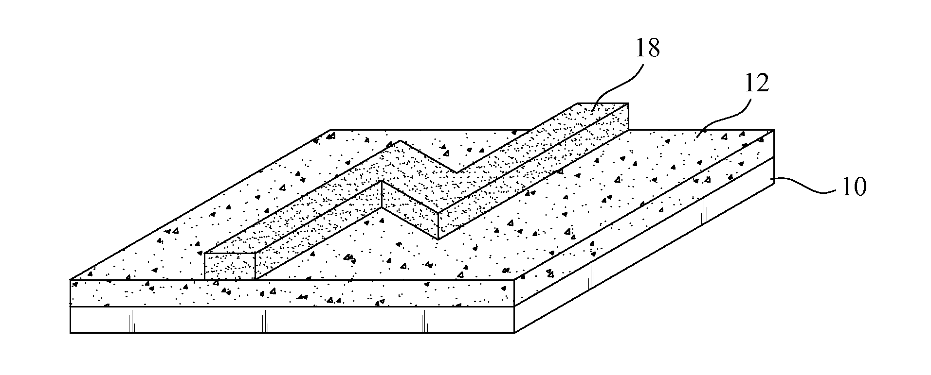
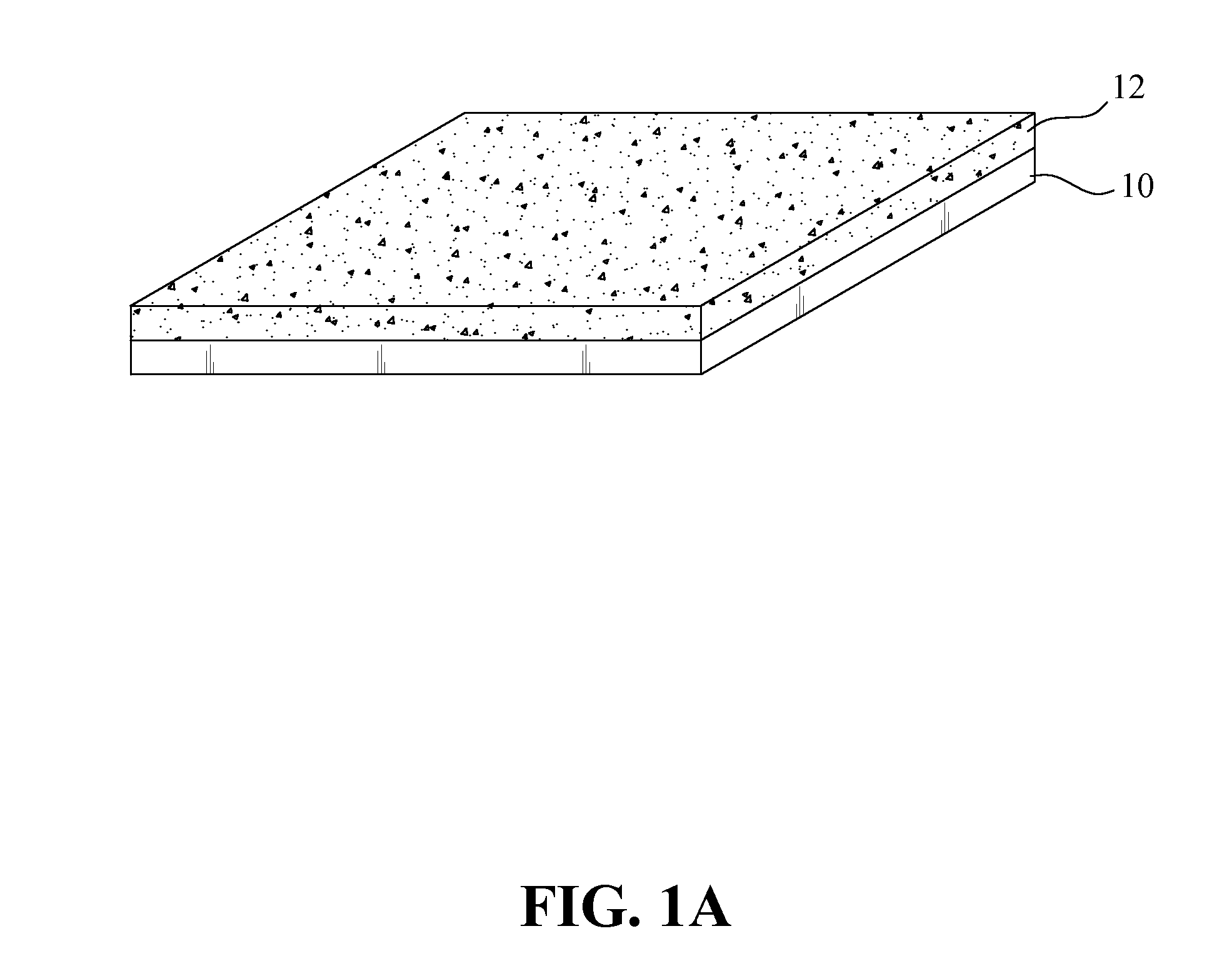
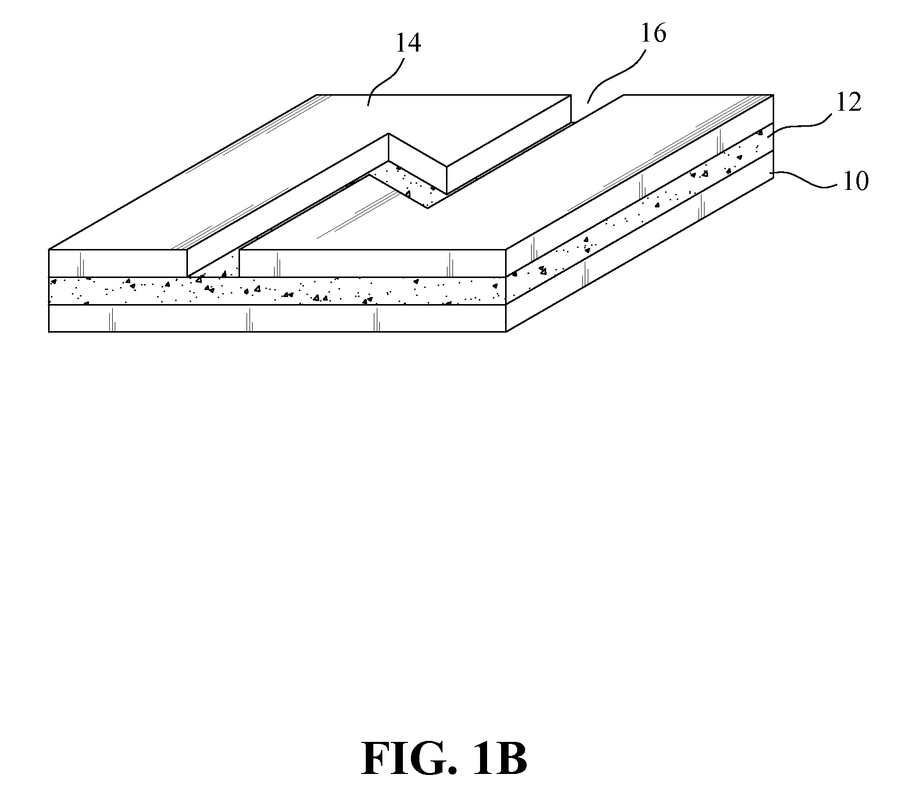
[0013]Referring to FIG. 1A, a substrate 10 is provided. Then, an adhesive material is coated on the substrate 10 to form an adhesive layer 12. As shown in FIG. 1B, a patterned mask 14 is formed on the adhesive layer 12. The patterned mask 14 has an opening 16 which defines a wiring pattern. The patterned mask 14 can be fabricated by forming an opening 16 in an insulating or a metallic plate.

[0014]As shown in FIG. 1C, an electrically conductive paste is filled in the opening 16 of the patterned mask 14 by the screen printing method to form the wiring pattern 18 (in other words, the wiring pattern 18 is transferred to the substrate 10 via the patterned mask 14). The electrically conductive paste can be an electrically conductive silver or copper paste.

[0015]Finally, as shown in FIG. 1D, the patterned mask 14 is removed.

[0016]As des...


PUM

PropertyMeasurementUnit
electrically conductiveaaaaaaaaaa
pHaaaaaaaaaa
temperatureaaaaaaaaaa

Abstract

A method of forming a wiring pattern is provided. In the method, an adhesive material is coated on a substrate to form an adhesive layer, and then a patterned mask is provided on the adhesive layer, wherein the patterned mask has an opening defining a wiring pattern, and then an electrically conductive paste is filled in the opening, and subsequently the patterned mask is removed so as to form the wiring pattern on the substrate. In the method of the present invention, a wiring pattern is formed by using a screen printing method, but not by using an etching method. As a result, there are no etching contamination issues. Furthermore, the difficulty in etching the finer wiring patterns from the copper foil can be alleviated.

Description

BACKGROUND OF THE INVENTION[0001]1. Field of the Invention[0002]The present invention relates to a method of forming a wiring pattern, and more particularly to a method of forming a wiring pattern using a screen printing method.[0003]2. The Prior Arts[0004]A printed circuit board usually comprises a wiring pattern that is formed of an electrically conductive material on an insulating material according to the circuit design. In the conventional method, a copper layer is formed on an insulating substrate, and then a desired pattern (for example, a wiring pattern, an alignment hole, a mark, etc.) is formed on the insulating substrate by the photolithography and etching methods.[0005]However, the current legislations for environment protection require that the highly contaminant byproducts formed during the etching process have to be recycled and properly treated, which increases the manufacture cost.[0006]Furthermore, in a chemical etching process, the accurate control of the pH value...

Claims


Application Information

Patent Timeline
Patent Type & Authority Applications(United States)
IPC IPC(8): H05K3/10H05K3/12
CPCH05K3/1216H05K3/1208
Inventor HO, CHIEN-HANHO, YEN-CHIH
Owner HO CHIEN HAN
Why Eureka
Try Eureka