Semiconductor device and method for forming the same

Inactive Publication Date: 2009-08-04
SEMICON ENERGY LAB CO LTD
View PDF197 Cites 6 Cited by
  • Summary
  • Abstract
  • Description
  • Claims
  • Application Information

AI Technical Summary

Benefits of technology

[0043]An offset region to which no electric field or very weak electric field is applied by a gate voltage can be formed in a portion of a channel region in contact with a source or a drain region in an insulated gate field effect transistor in which a channel length thereof is longer than a length of a gate electrode thereof in a direction of the channel length. For example, in FIG. 5, no electric field is applied to the offset region located in the channel region in the semiconductor 102 betwe

Problems solved by technology

As mentioned earlier, the TFTs fabricated by a thin film deposition process at low temperatures are significantly low in the carrier mobility.
Even upon doping an impurity, the still low conductivity produces a resistance within this distance L. Accordingly, the conventional TFTs suffer poor frequency characteristics and increase in ON circuit resistance.
Furthermore, the area necessary for a TFT increases inevitably with increasing length of L. This made it difficult to accommodate a predetermi

Method used


Image

  • Semiconductor device and method for forming the same
  • Semiconductor device and method for forming the same
  • Semiconductor device and method for forming the same

Examples


example 1

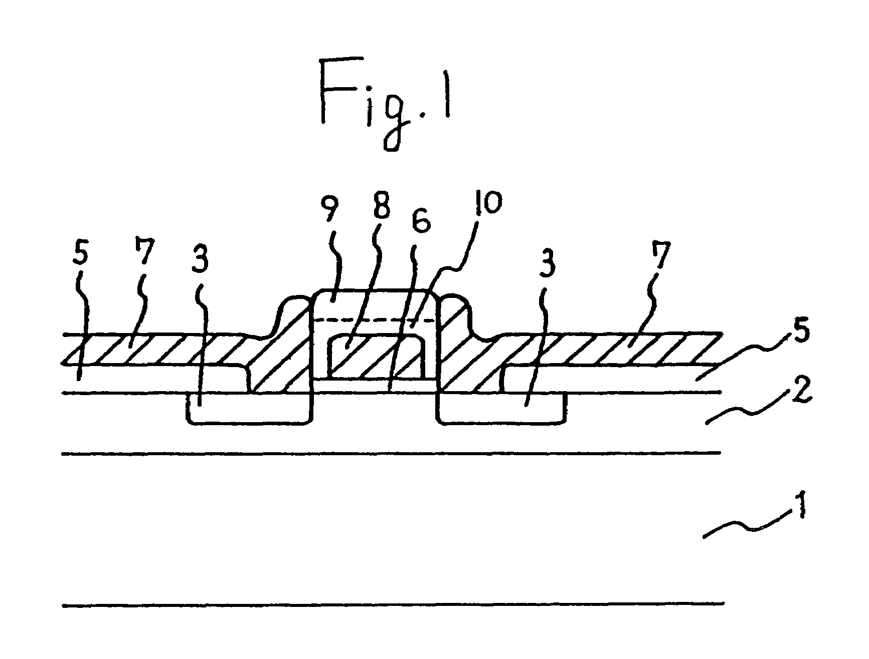
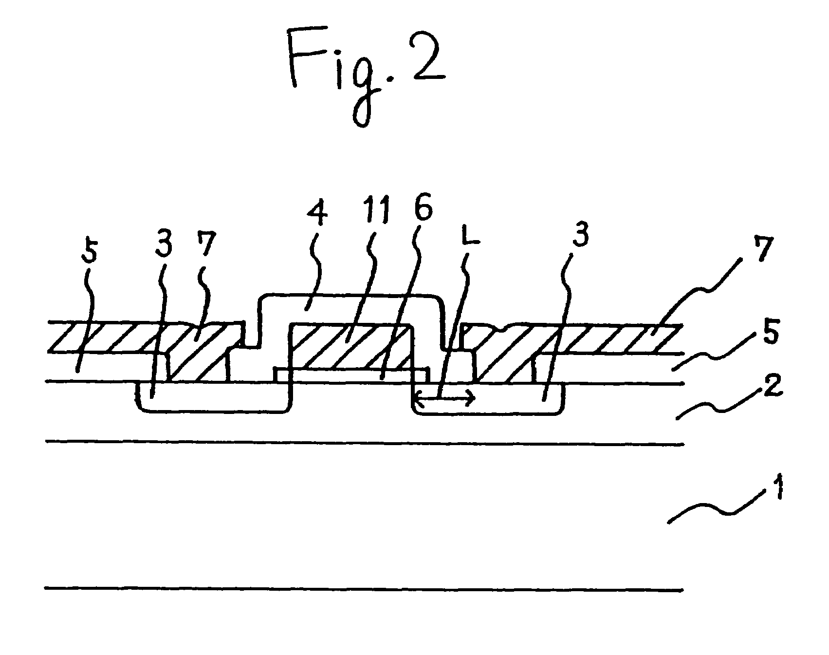
[0059]Referring to FIG. 4, an example in which a TFT according to the present invention is applied to a liquid crystal electro-optical device having a diagram as illustrated i FIG. 4 is described. In FIG. 4, an N-channel TFT (N-TFT) 22 and a P-channel TFT (P-TFT) 21 in a complementary configuration are provided to each of the pixels of the liquid crystal device. Each of the TFTs are connected to a common signal wire 50 through respective gate electrodes, and the output terminals of the N-TFT 22 and the P-TFT 21 are connected to the common pixel electrode 43, whereas each of the other output terminals 28 and 35 in the respective TFTs is connected to the other signal wires 52 and 53 to provide an inverter structure. The positions of the P-TFT and the N-TFT may be reversed to establish a buffer structure and provide the complementary TFTs to each of the pixel electrodes.

[0060]Referring to FIGS. 3(A) to 3(G), the fabrication process of a complementary TFT (C / TFT) on a substrate accordin...

example 2

[0102]Referring to FIG. 10, an example of an active matrix type liquid crystal electro-optical device to which a TFT according to the present invention is applied is described. FIG. 10 shows the circuit diagram of the liquid crystal electro-optical device, and it can be seen therefrom that the active elements of the present EXAMPLE are provided in a complementary arrangement having a P-TFT and an N-TFT per one pixel contact.

[0103]The actual arrangement of the contacts and the like corresponding to the circuit shown in FIG. 10 is given in FIG. 12. For brevity's sake, merely a part of the circuit corresponding to a 2×2 matrix is given in FIG. 12.

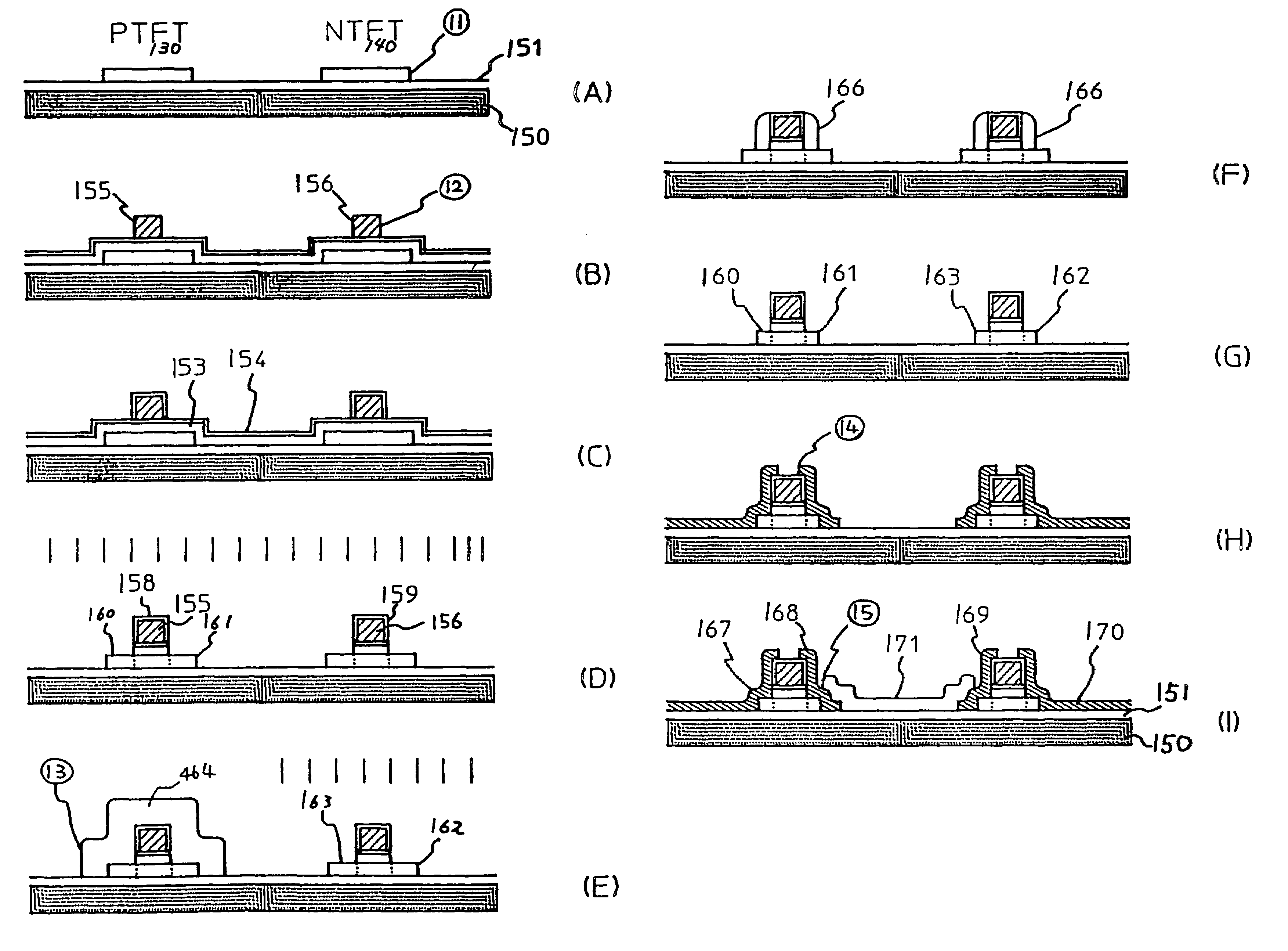
[0104]Referring first to FIG. 11, the process for fabricating the substrate for use in the liquid crystal electro-optical device according to the present invention is described. FIG. 11(A) shows a step of depositing silicon oxide film as a blocking layer 151 at a thickness of from 1000 to 3000 Å, on a non-expensive glass substrate 150 using RF...

example 3

[0133]Referring to FIG. 13, an example of a liquid crystal electro-optical device comprising pixels having provided to each thereof modified transfer-gate TFTs in a complementary arrangement is described. The TFTs in this EXAMPLE are fabricated basically in the same process as those in EXAMPLE 2, and the process steps proceed in a similar manner as shown in FIG. 11. The only difference is the arrangement of the C / TFT shown in FIG. 11, because the one used in the present EXAMPLE is a modified transfer-gate C / TFT. The actual arrangement and connection of the C / TFT of the present EXAMPLE is given in FIG. 14.

[0134]As shown in FIG. 13, a common gate wire 191 is connected with gates of a P-TFT 195 and a N-TFT 196. These TFTs are connected to another signal wire 193 through source and drain areas, and the other source and drain areas are connected to a common pixel electrode.

[0135]The fabrication process proceeds the same to FIG. 11(G). The structure obtained to the step shown in FIG. 11(G...


PUM


Abstract

An insulated gate field effect semiconductor device comprising a substrate having provided thereon a thin-film structured insulated gate field effect semiconductor device, said device being characterized by that it comprises a metal gate electrode and at least the side thereof is coated with an oxide of the metal. The insulated gate field effect semiconductor device according to the present invention is also characterized by that the contact holes for the extracting contacts of the source and drain regions are provided at about the same position of the end face of the anodically oxidized film established at the side of the gate. Furthermore, the present invention provides a method for forming insulated gate field effect semiconductor devices using less masks.

Description

[0001]This is a Divisional application of Ser. No. 08 / 504,225, filed Jul. 19, 1995, now abandoned which is a divisional application of Ser. No. 08 / 147,580, filed Nov. 5, 1993, now U.S. Pat. No. 5,474,945, which in turn is a divisional application of Ser. No. 07 / 846,164, filed Mar. 5, 1992, now U.S. Pat. No. 5,289,030.BACKGROUND OF THE INVENTION[0002]1. Field of the Invention[0003]The present invention relates to a semiconductor device and a method for forming the same. More particularly, the present invention relates to a thin film transistor applicable to liquid crystal electro-optical devices, contact type image sensors, and the like.[0004]2. Description of the Prior Art[0005]Insulated gate field effect semiconductor devices known to the present have been widely applied to various fields. Such semiconductor devices comprise a silicon substrate having integrated thereon a plurality of semiconductor elements so that the devices may function as integrated circuits (ICs) and large sca...

Claims


Application Information

Patent Timeline
IPC IPC(8): H01L21/00G02F1/1362H01L21/336H01L21/60H01L27/12H01L29/49H01L29/786
CPCH01L21/76897H01L27/12H01L29/66757H01L29/78651H01L29/78666H01L29/78675H01L29/4908G02F1/13454G02F2001/136245Y10S257/90G02F1/136245H01L29/78H01L21/18
Inventor YAMAZAKI, SHUNPEIMASE, AKIRAHAMATANI, TOSHIJI
Owner SEMICON ENERGY LAB CO LTD
Why Eureka
Try Eureka