Method for manufacturing ferroelectric memory device

a technology of ferroelectric memory and manufacturing method, which is applied in the direction of semiconductor devices, capacitors, electrical apparatus, etc., can solve the problems of difficult to obtain favorable ferroelectric characteristics, difficult to be patterned, and titanium oxides cannot be used as hard masks, etc., and achieves the effect of increasing resistance and electrical conductivity

Inactive Publication Date: 2007-09-20
SEIKO EPSON CORP
View PDF5 Cites 1 Cited by
  • Summary
  • Abstract
  • Description
  • Claims
  • Application Information

AI Technical Summary

Benefits of technology

[0019]Because the oxygen barrier film is formed between the base substrate and the lower electrode, oxidation of a plug formed in the base substrate and the resultant substantial increase in its resistance in a heat treatment that may be conducted in an ...

Problems solved by technology

As masks that are used for etching, hard masks such as oxide (e.g., SiO2) films are used more in recent years, because resist masks cannot provide sufficient etching resistance (see, for example, Japanese laid-open patent application JP-A-2002-94019).
However, when over-etching is conducted excessively, sidewall surfaces ...

Method used


Image

  • Method for manufacturing ferroelectric memory device
  • Method for manufacturing ferroelectric memory device
  • Method for manufacturing ferroelectric memory device

Examples


Embodiment Construction

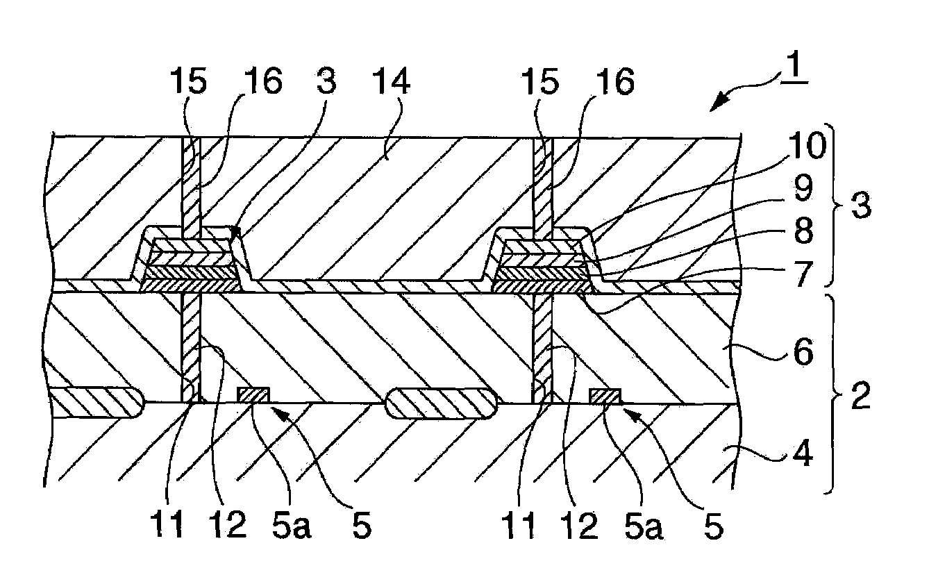
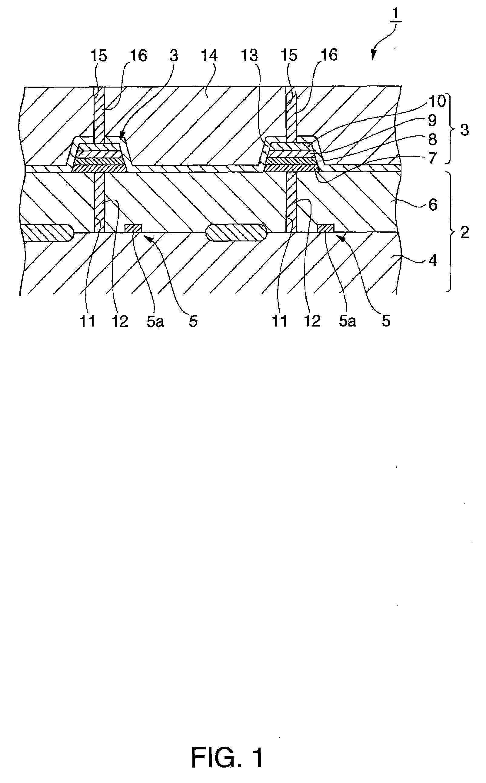
[0025]Preferred embodiments of the invention are described in detail below. Prior to description of a method for manufacturing a ferroelectric memory device in accordance with an embodiment of the invention, an example of the ferroelectric memory device obtained by the method is described.

[0026]FIG. 1 is a cross-sectional view in part of a ferroelectric memory device in accordance with an embodiment of the invention. Reference numeral 1 in the figure denotes a ferroelectric memory device. The ferroelectric memory device 1 is of a stacked type having a 1T / 1C memory cell structure, and is equipped with a base substrate 2, and a plurality of ferroelectric capacitors 3 provided on the base substrate 2.

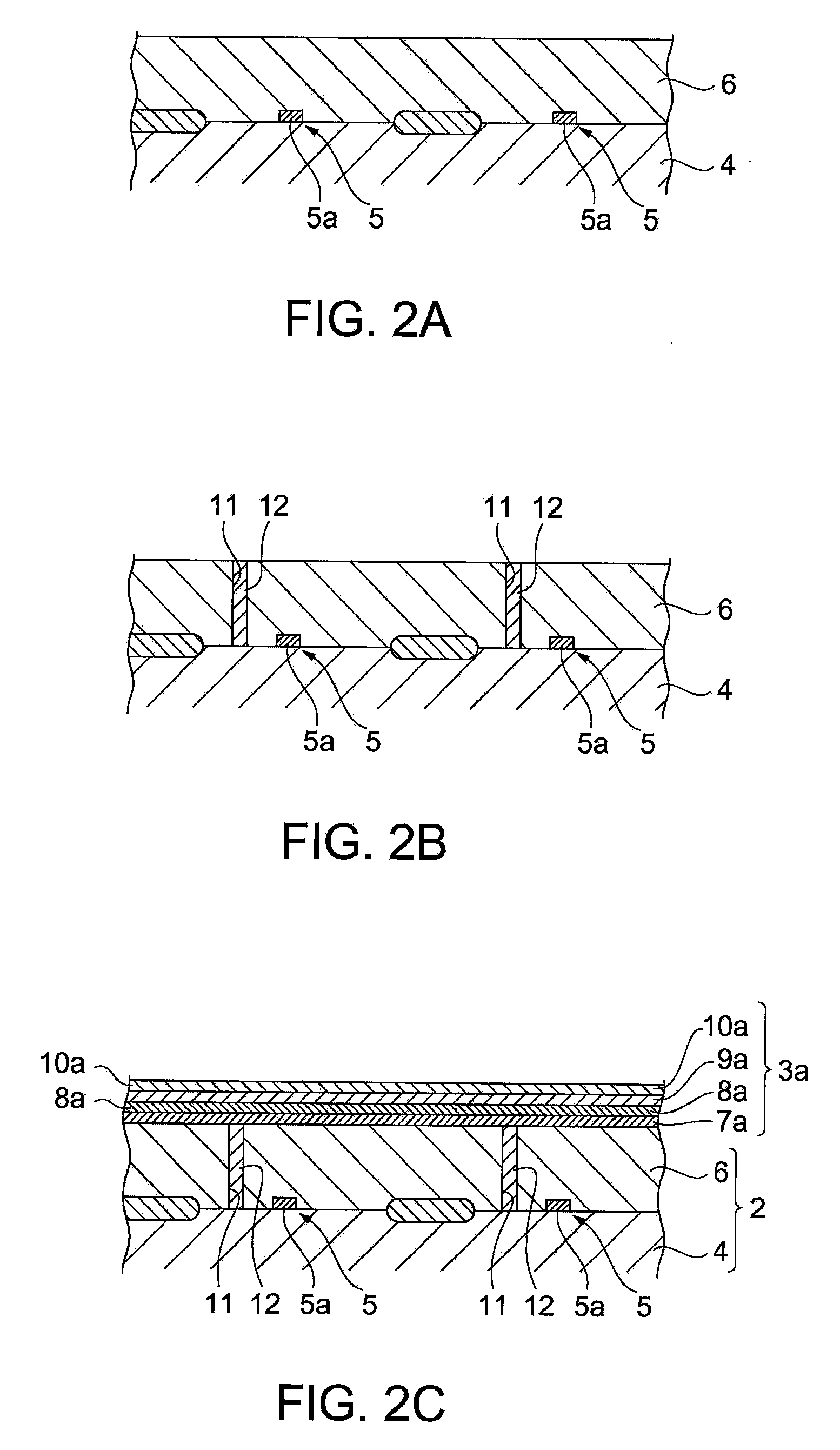
[0027]The base substrate 2 is formed from a silicon substrate (i.e., a semiconductor substrate) 4. Transistors 5 for driving the ferroelectric capacitors 4 are formed on a top surface portion of the silicon substrate 4, and a base dielectric film 6 that covers the driving transistors 5 is ...


PUM


Abstract

A method for manufacturing a ferroelectric capacitor, includes the steps of: forming a ferroelectric capacitor layer having a lower electrode layer, a ferroelectric layer and an upper electrode layer on a base substrate; forming a titanium oxide layer on the ferroelectric capacitor layer; patterning the titanium oxide layer by high-temperature etching between 200° C. and 500° C. to thereby form a mask pattern; and etching the ferroelectric capacitor layer by using the mask pattern as a mask, to thereby form a ferroelectric capacitor having a lower electrode, a ferroelectric film and an upper electrode.

Description

[0001]The entire disclosure of Japanese Patent Application No. 2006-064011, filed Mar. 9, 2006 is expressly incorporated by reference herein.BACKGROUND[0002]1. Technical Field[0003]The present invention relates to methods for manufacturing ferroelectric memory devices having ferroelectric capacitors.[0004]2. Related Art[0005]A ferroelectric memory device (FeRAM) is composed with ferroelectric capacitors, and is a nonvolatile memory that is capable of low voltage and high speed operations. In such a ferroelectric memory device, its memory cell can be composed of, for example, one transistor and one capacitor (1T / 1C), such that integration to the level of DRAM is possible. Accordingly, ferroelectric memory devices are highly expected as large capacity nonvolatile memories in recent years.[0006]A ferroelectric capacitor in such a ferroelectric memory device is formed from a lower electrode, a ferroelectric film and an upper electrode. When the ferroelectric capacitor is formed, normall...

Claims


Application Information

Patent Timeline
IPC IPC(8): H01L21/00H01L21/8242
CPCH01L27/11502H01L28/65H01L28/57H01L27/11507H10B53/30H10B53/00
Inventor MIYAJI, MAMORU
Owner SEIKO EPSON CORP
Why Eureka
Try Eureka