Semiconductor device

a semiconductor device and semiconductor technology, applied in the field of semiconductor devices, can solve the problems of inability to implement miniaturization of semiconductor devices and penalty for area, and achieve the effect of preventing the generation of area penalties and contact defects

Inactive Publication Date: 2004-07-20
RENESAS TECH CORP
View PDF7 Cites 6 Cited by
  • Summary
  • Abstract
  • Description
  • Claims
  • Application Information

AI Technical Summary

Benefits of technology

Therefore, an object of the present invention is to solve the above described problem and to provide a semiconductor device wherein contact defects in the upper electrode are prevented and the generation of an area penalty is prevented.
In addition, the sidewall of the upper electrode defined by the first hole does not have a depth greater than a constant depth. Therefore, the upper electrode can be provided with a stable contact resistance between the upper electrode and the conductive film filled into the first hole. Furthermore, contact defects of the upper electrode are prevented through the formation of the upper electrode of predetermined materials, instead of relying upon the specific structure. Accordingly, no area penalty is produced so that miniaturization of the semiconductor device can be implemented.
In addition, the first hole is formed in a manner that does not allow penetration beyond the upper electrode. Therefore, there is no risk of the first hole reaching a wire film or the like, separately provided from the upper electrode so that the conductive film filled into the first hole and this wire film form a short circuit. In addition, the bottom of the first hole is defined by the upper electrode, except for the case where the distance between the main surface of the semiconductor substrate and the bottom face of the first hole is equal to the distance between the main surface of the semiconductor substrate and the bottom face of the upper electrode. Therefore, the area of contact between the conductive film filled into the first hole and the upper electrode increases so that contact defects due to small contact area can be prevented.
According to the semiconductor device having such a configuration, in the case that the interlayer insulating film is etched so that the first hole and second hole, which is deeper than the first hole, are simultaneously formed, the upper electrode continues to undergo etching after the first hole has reached the top face of the upper electrode. However, the etchant for removal of portions of the interlayer insulating film etches the upper electrode at a relatively low etching rate and, therefore, it is difficult to etch the upper electrode when the interlayer insulating film is etched. Therefore, even when the upper electrode continues to undergo etching, etching stops at a predetermined position of the upper electrode so that the first hole is formed in a manner that does not allow penetration beyond the upper electrode. Thereby, the desired contact structure between the upper electrode and the conductive film filled into the first hole can be obtained.

Problems solved by technology

The term area penalty indicates a disadvantage caused by usage of space above a semiconductor substrate wherein a structure is provided in order to achieve a specific purpose.
Therefore, a problem arises wherein the area of the memory cell region increases, so that miniaturization of the semiconductor device cannot be implemented.
Therefore, a problem arises wherein the contact resistance between metal contact 211 and capacitance electrode 210 is dispersed.

Method used


Image

  • Semiconductor device
  • Semiconductor device
  • Semiconductor device

Examples


tenth embodiment

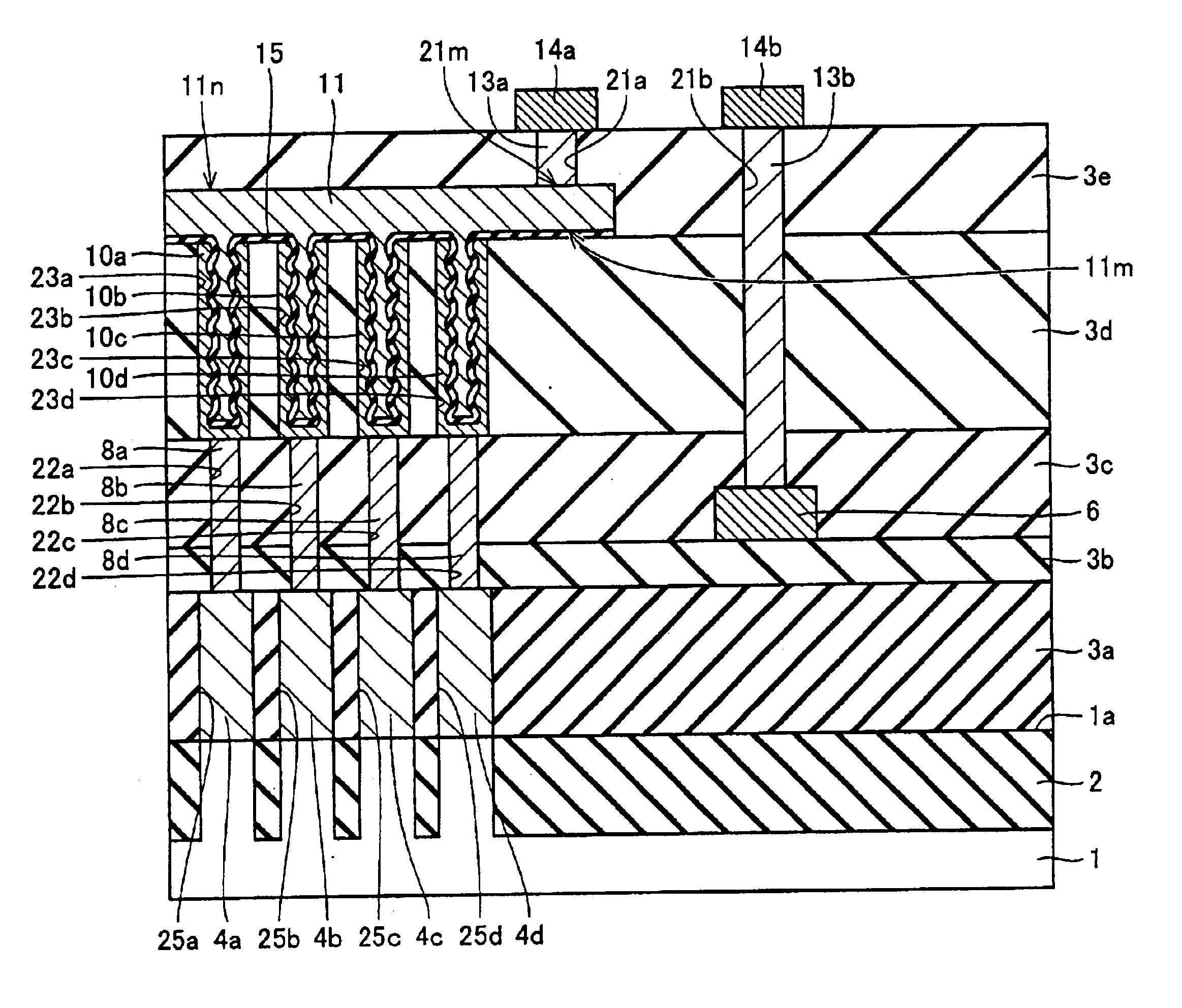
The capacitor structure of the semiconductor device according to a tenth embodiment differs from that of the semiconductor device according to the first embodiment, and that is the only difference between the two. In the following, the same structures will not be described repeatedly.

With reference to FIG. 18 a semiconductor device has a concave MIM (metal-insulator-metal) capacitor. Holes 23a to 23d are formed in fourth interlayer insulating film 3d so as to reach the respective top faces of storage node contacts 8a to 8d. Lower storage node electrodes 10a to 10d made of ruthenium (Ru) are formed in holes 23a to 23d so as to cover the bottoms and the sidewalls of holes 23a to 23d. Furthermore, recesses are formed in lower storage node electrodes 10a to 10d, located in holes 23a to 23d, and the surfaces resulting from the formation of these recesses are flat.

A dielectric film 15 made of tantalum oxide (Ta.sub.2 O.sub.5) or barium strontium tantalum oxide (BST) is formed so as to cov...

eleventh embodiment

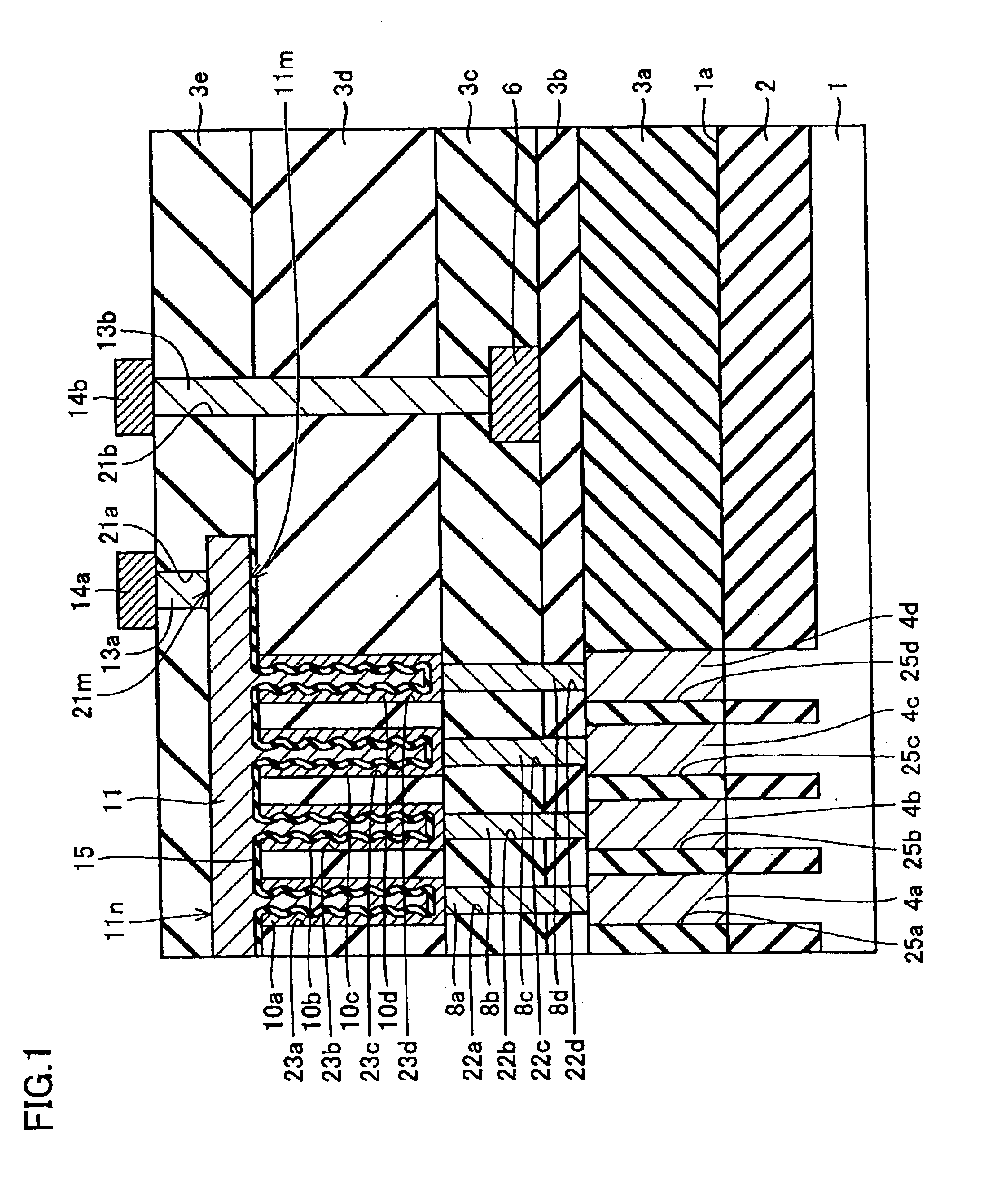
The capacitor structure of the semiconductor device according to an eleventh embodiment differs from that of the semiconductor device according to the second embodiment, and that is the only difference between the two. With reference to FIG. 19 the semiconductor device has a concave MIM (metal-insulator-metal) capacitor as described in the tenth embodiment.

According to the semiconductor device having such a configuration, the same effects as the effects according to the second embodiment can be obtained.

twelfth embodiment

The capacitor structure of the semiconductor device according to a twelfth embodiment differs from that of the semiconductor device according to the third embodiment, and that is the only difference between the two. With reference to FIG. 20 the semiconductor device has a concave MIM (metal-insulator-metal) capacitor as described in the tenth embodiment.

According to the semiconductor device having such a configuration, the same effects as the effects according to the third embodiment can be obtained.


PUM


Abstract

A semiconductor device includes: lower storage node electrodes provided on a main surface of a silicon substrate; a dielectric film provided on the lower storage node electrodes; an upper cell plate electrode provided on the dielectric film; and an interlayer insulating film covering the upper cell plate electrode. The upper cell plate electrode contains ruthenium. The interlayer insulating film has a contact hole reaching the upper cell plate electrode. The contact hole is provided so that the distance between the main surface of the silicon substrate and the bottom face of the contact hole is not less than the distance between the main surface of the silicon substrate and the bottom face of the upper cell plate electrode. A semiconductor device is provided wherein contact defects in the upper electrode and the generation of an area penalty are prevented.

Description

BACKGROUND OF THE INVENTION1. Field of the InventionThe present invention generally relates to a semiconductor device, and more particularly to a semiconductor device with a capacitor.2. Description of the Background ArtIn recent years, a cylindrical capacitor structure wherein the effective area of an actual capacitor can be made large relative to the projection area of the memory cell has been widely used while, at the same time, miniaturization of the structure of semiconductor devices, in particular of DRAMs (dynamic random access memories), has proceeded. Such a cylindrical capacitor structure has a layered structure provided with a lower electrode formed in a cylinder, a dielectric film covering the surface of the lower electrode and a cell plate. FIG. 54 is a cross sectional view showing a semiconductor device having a cylindrical capacitor structure according to prior art.With reference to FIG. 54, gate electrodes 104a to 104c are formed above the main surface 101a of a semi...

Claims


Application Information

Patent Timeline
Patent Type & Authority Patents(United States)
IPC IPC(8): H01L21/70H01L27/108H01L29/66H01L29/76H01L21/8242H01L21/768H01L21/108
CPCH01L27/10894H01L27/10814H01L27/10882H10B12/315H10B12/48H10B12/09H01L21/108
Inventor TAKEUCHI, MASAHIKODOKAN, TAKASHI
Owner RENESAS TECH CORP
Why Eureka
Try Eureka