Multi-radiofrequency impedance control for plasma uniformity tuning

a radiofrequency impedance control and uniformity tuning technology, applied in the field of wafer processing equipment, can solve the problems of limiting the control of the desired process chemistry, unable to control the ion energy in the chamber, and difficulty in accommodating all the applications in the same processing equipment without adequate controls

Active Publication Date: 2013-10-03
LAM RES CORP
View PDF11 Cites 52 Cited by
  • Summary
  • Abstract
  • Description
  • Claims
  • Application Information

AI Technical Summary

Benefits of technology

[0010]In one embodiment, a wafer processing apparatus includes top and bottom electrodes of a processing chamber, a first radio frequency (RF) power source, a second RF power source, a third RF power source, a fourth RF power source, and one or more resonant circuits. The first, second, and third RF power sources are coupled to the bottom electrode. The top electrode may be coupled to the fourth RF power source, to electrical ground, or to the one or more resonant circuits. Each of the one or more resonant circuits resonate at one of the frequencies of the RF power sources coupled to the bottom electrode. In one embodiment, a first resonant is coupled between the top electrode and electrical ground, the first resonant circuit including a tune-in element operable to vary a frequency dependent impedance of the first resonant circuit. The wafer processing apparatus is configurable to select the RF power sources for wafer processing operations, as well as the connections to the top electrode in order to provide plasma and etching uniformity for the wafer.

Problems solved by technology

Unfortunately, chemistry dissociation and radical formation are coupled to ion production and plasma density and often do not work in concert to achieve the desired plasma processing conditions.
However the requirements for each of the applications may vary substantially, and it may be difficult to accommodate all the applications in the same processing equipment without adequate controls to configure the wafer processing process (e.g., to control the plasma chemistry in the chamber).
A lack of control on the ion energy in the chamber limits the control of the desired process chemistry.
If controls are not adequate, non-uniform deposition may result with non-uniform etching on the wafer.

Method used


Image

  • Multi-radiofrequency impedance control for plasma uniformity tuning
  • Multi-radiofrequency impedance control for plasma uniformity tuning
  • Multi-radiofrequency impedance control for plasma uniformity tuning

Examples


Embodiment Construction

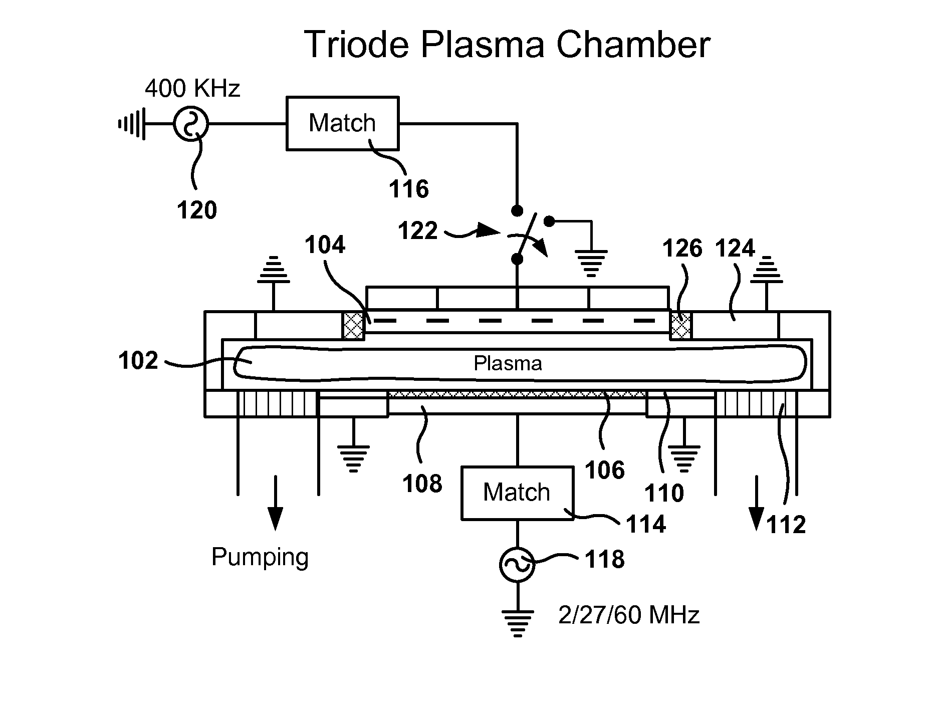
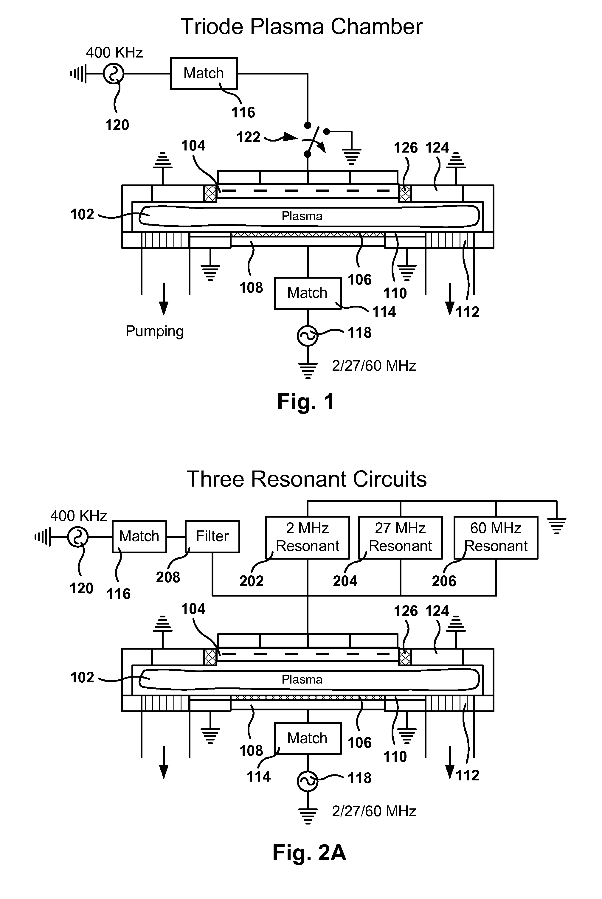
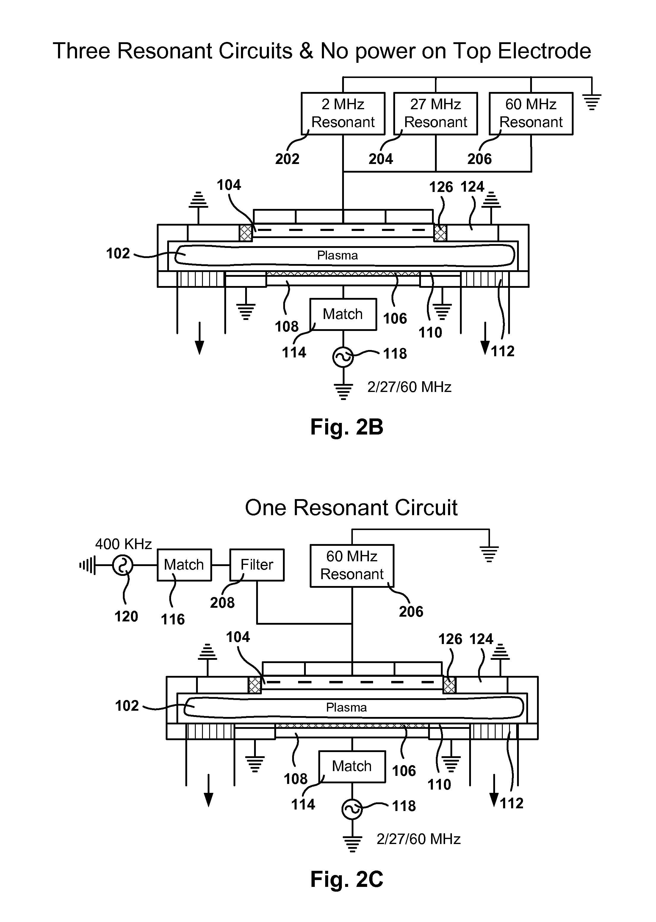
[0025]The following embodiments describe apparatus, methods and computer programs for processing a wafer in a wafer processing apparatus. Embodiments of the disclosure use up to four different RF powers in a triode reactor configuration and one or more resonant circuits coupled to the top electrode. It will be apparent, that the present embodiments may be practiced without some or all of these specific details. In other instances, well known process operations have not been described in detail in order not to unnecessarily obscure the present embodiments.

[0026]FIG. 1 shows an etching chamber, according to one embodiment. Exciting an electric field between two electrodes is one of the methods to obtain RF gas discharge in an etching chamber. When an oscillating voltage is applied between the electrodes, the discharge obtained is referred to as a Capacitive Coupled Plasma (CCP) discharge.

[0027]Plasma can be created utilizing stable feedstock gases to obtain a wide variety of chemicall...


PUM

PropertyMeasurementUnit
frequencyaaaaaaaaaa
frequencyaaaaaaaaaa
frequencyaaaaaaaaaa

Abstract

Circuits, methods, chambers, systems, and computer programs are presented for processing wafers. A wafer processing apparatus includes top and bottom electrodes inside a processing chamber; a first, second, third, and fourth radio frequency (RF) power sources; and one or more resonant circuits. The first, second, and third RF power sources are coupled to the bottom electrode. The top electrode may be coupled to the fourth RF power source, to electrical ground, or to the one or more resonant circuits. Each of the one or more resonant circuits, which are coupled between the top electrode and electrical ground, include a tune-in element operable to vary a frequency-dependent impedance presented by the resonant circuit. The wafer processing apparatus is configurable to select the RF power sources for wafer processing operations, as well as the connections to the top electrode in order to provide plasma and etching uniformity for the wafer.

Description

CROSS REFERENCE TO RELATED APPLICATIONS[0001]This application is related by subject matter to U.S. patent application Ser. No. 13 / 301,725 filed Nov. 21, 2011, and entitled “TRIODE REACTOR DESIGN WITH MULTIPLE RADIOFREQUENCY POWERS”, all of which is incorporated herein by reference.BACKGROUND[0002]1. Field of the Invention[0003]The present embodiments relate to wafer processing apparatus, and more particularly, apparatus, methods, and computer programs for processing a wafer in a wafer processing apparatus.[0004]2. Description of the Related Art[0005]The manufacturing of integrated circuits includes immersing silicon substrates (wafers) containing regions of doped silicon into chemically-reactive plasmas, where the submicron device features (e.g., transistors, capacitors, etc.) are etched onto the surface. Once the first layer is manufactured, several insulating (dielectric) layers are built on top of the first layer, where holes, also referred to as vias, and trenches are etched int...

Claims


Application Information

Patent Timeline
Patent Type & Authority Applications(United States)
IPC IPC(8): H01L21/3065
CPCH01J37/32165H01J37/32091H01L21/3065H03H7/40H05H1/46
Inventor MARAKHTANOV, ALEXEIDHINDSA, RAJINDER
Owner LAM RES CORP
Why Eureka
Try Eureka