Nanowire field-effect device with multiple gates

a field-effect device and nanowire technology, applied in the field of nanowire field-effect devices, can solve the problems of process incompatibilities and deterioration of the tunneling efficiency of carriers, and achieve the effects of reducing the band gap improving the tunneling efficiency of carriers, and reducing the barrier height of the tunnel junction between the source region and the channel region

Inactive Publication Date: 2013-10-10
IBM CORP
View PDF4 Cites 22 Cited by
  • Summary
  • Abstract
  • Description
  • Claims
  • Application Information

AI Technical Summary

Benefits of technology

[0011]According to an embodiment of a first aspect of the present invention, there is provided a semiconductor device comprising: at least a nanowire configured to comprise: at least a source region comprising a corresponding source semiconductor material, at least a drain region comprising a corresponding drain semiconductor material and at least a channel region comprising a corresponding channel semiconductor material, the channel region being arranged between the source region and the drain region, at least a gate electrode that is arranged relative to the nanowire to circumferentially surround at least a part of the channel region, and at least a strain gate that is arranged relative to the nanowire to circumferentially surround at least a part of a segment of the nanowire, the strain gate being configured to apply a strain to the nanowire segment, thereby to facilitate at least an alteration of the energy bands corresponding to the source region relative to the energy bands corresponding to the channel region. Due to the strain application feature in an embodiment of the present invention, an alteration of the energy-bands corresponding to the source region relative to the energy-bands corresponding to the channel region may be facilitated. Particularly, by way of the strain application to the nanowire segment, the band-gap of the semiconductor material corresponding thereto may be altered and, more desirably, reduced. This has the corresponding effect of altering the band-alignment of the energy-bands corresponding to the source region and the energy-bands corresponding to the channel region—desirably, the band-alignment between the energy-bands of the source region and the channel region is altered such that the band-gap of the source region is reduced compared to that of the channel region. In this way, the barrier height of the tunnel junction between the source region and the channel region may be reduced, thereby improving the tunneling efficiency of carriers across the tunnel junction in an embodiment of the present invention as compared to previously-proposed devices. A tunneling mass of carriers across the tunneling junction may be altered in addition to, or independently of, the band-gap reduction of the source region by the strain application, which facilitates an improved tunneling rate of carriers across the tunnel junction, thereby contributing to an improved tunneling efficiency of an embodiment of the present invention compared to previously-proposed devices. Alteration of the tunneling mass of the carriers may be facilitated by altering a curvature of the energy-bands corresponding to the source region relative to the curvature of the energy-bands corresponding to the channel region.
[0012]Preferably, the strain gate is configurable to apply a strain gate bias to the nanowire segment, thereby to facilitate electrostatic doping of the nanowire segment. An embodiment of the present invention may be configured to apply a strain gate bias to the nanowire segment via the strain gate. By appropriate selection of the strain gate bias, the semiconductor material corresponding to the nanowire segment may be doped with a desired polarity of carriers. In this way, electrostatic doping of the nanowire segment may be facilitated. An advantage associated with electrostatic doping according to an embodiment of the present invention is that doping may be performed without substantially any chemical impurities and / or implantation process. A further advantage associated with electrostatic doping is it entails no thermal treatment for the activation of dopants—such thermal treatment may cause diffusive widening of the doped areas and, therefore, a tunnel junction with a “smeared” tunnel junction. The latter feature is, of course, undesirable since it may cause a deterioration of the tunneling efficiency of carriers across the tunnel junction. Thermal treatments for doping also cause process incompatibilities—this problem is bypassed in electrostatic doping. Furthermore, in a vertical process, the doping problems associated thereto, such as, for example, the difficulty in implanting dopant in the nanowire, may be bypassed by electrostatic doping according to an embodiment of the present invention. For some semiconductor material systems, such as, for example, III-V compound semiconductors, electrostatic doping may present relatively significant design and / or processing advantages since: the impurity doping of one or both polarities of III-V semiconductor systems may be challenging as compared to the case for Si; it may be challenging to achieve sufficient activated dopants of either polarity in such material systems by known doping methods and such material systems have relatively narrow temperature constraints.
[0013]Preferably, the strain gate comprises a material that is chosen to provide a specific strain value to the nanowire segment and to have a work-function value in accordance with a polarity of the semiconductor device. This feature provides the advantage that the strain gate may be configured to perform the dual function of strain application and electrostatic doping of the nanowire segment.

Problems solved by technology

The latter feature is, of course, undesirable since it may cause a deterioration of the tunneling efficiency of carriers across the tunnel junction.
Thermal treatments for doping also cause process incompatibilities—this problem is bypassed in electrostatic doping.

Method used


Image

  • Nanowire field-effect device with multiple gates
  • Nanowire field-effect device with multiple gates
  • Nanowire field-effect device with multiple gates

Examples


Embodiment Construction

[0028]Within the description, the same reference numerals or signs have been used to denote the same parts or the like.

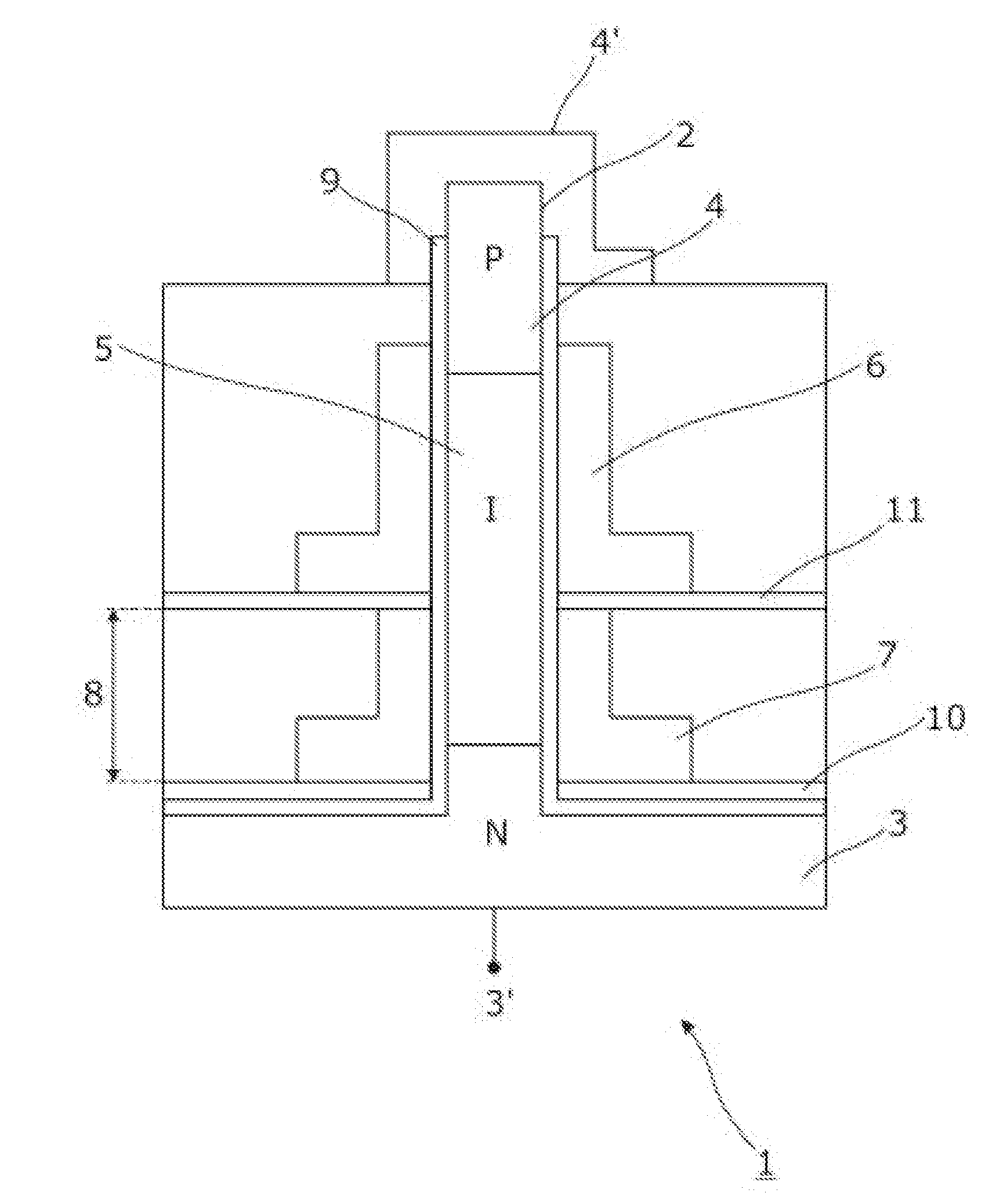
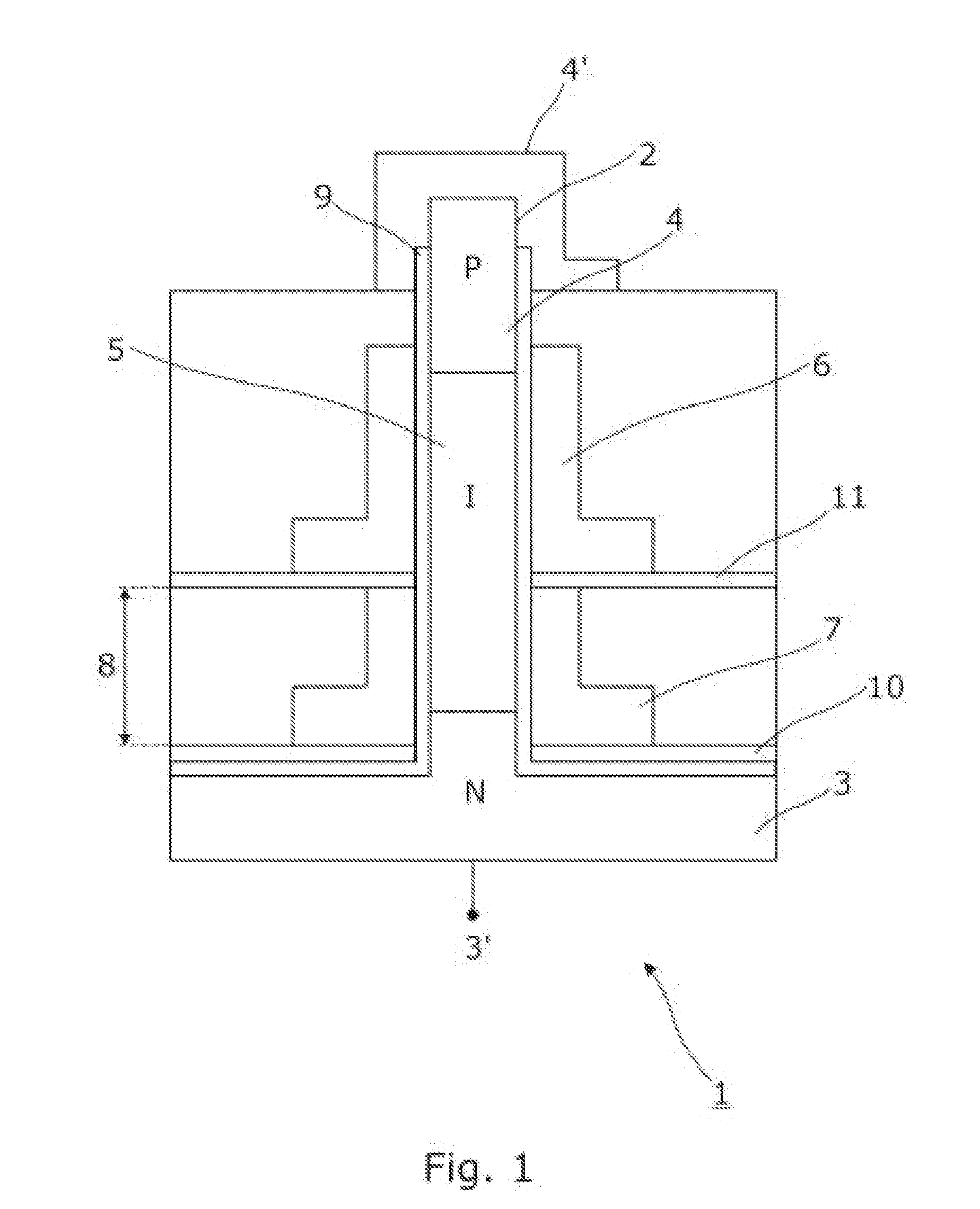
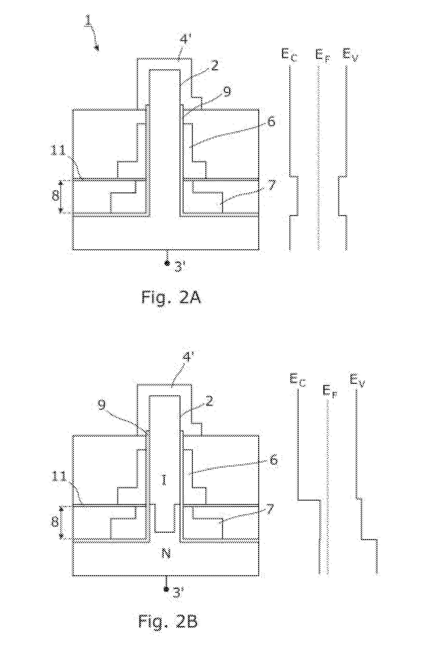
[0029]Reference is now made to FIG. 1, which schematically illustrates an embodiment according to a device aspect of the present invention.

[0030]As can be seen from FIG. 1, an embodiment of the present invention comprises a tunnel FET 1 that may be implemented by way of a nanowire 2. In this particular example of an embodiment of the present invention, the nanowire 2 is substantially vertically aligned and grown / etched out of an intrinsic semiconductor substrate. The nanowire 2 is configured to have at least three distinct regions: at least a source region 3 comprising a corresponding source semiconductor material, at least a drain region 4 comprising a corresponding drain semiconductor material and at least a channel region 5 comprising a corresponding channel semiconductor material that is disposed between the source region 3 and the drain region 4. As can be seen...


PUM


Abstract

The present invention relates to a semiconductor device (1) comprising: at least a nanowire (2) configured to comprise: at least a source region (3) comprising a corresponding source semiconductor material, at least a drain region (4) comprising a corresponding drain semiconductor material and at least a channel region (5) comprising a corresponding channel semiconductor material, the channel region (5) being arranged between the source region (3) and the drain region (4), at least a gate electrode (6) that is arranged relative to the nanowire (2) to circumferentially surround at least a part of the channel region (5), and at least a strain gate (7) that is arranged relative to the nanowire (2) to circumferentially surround at least a part of a segment of the nanowire (2), the strain gate (7) being configured to apply a strain to the nanowire segment (8), thereby to facilitate at least an alteration of the energy bands corresponding to the source region (3) relative to the energy bands corresponding to the channel region (5).

Description

FIELD OF THE INVENTION [0001]The present invention relates to a semiconductor device and a method of fabrication therefor.BACKGROUND OF THE INVENTION[0002]Tunnel field-effect transistors (FETs) may be used in several applications, including high-speed switching and logic circuits. Unlike the case for other types of FETs, an inverse sub-threshold slope of tunnel FETs is not limited to the 60 mV / dec at room temperature as determined by the Boltzmann tail of the Fermi statistics. Thus, tunnel FETS may potentially have a faster turn-on than previously-proposed devices, i.e. the bias range to facilitate the transition from an “ON”, conducting state, to an “OFF”, non-conducting state is smaller than is the case for previously-proposed devices, and both threshold and operating voltages may be reduced without a corresponding deterioration of device performance. This makes tunnel FETs particularly suitable for applications where reduced power consumption is desired.[0003]Until recently, the ...

Claims


Application Information

Patent Timeline
Patent Type & Authority Applications(United States)
IPC IPC(8): H01L29/775H01L29/66
CPCB82Y10/00B82Y40/00H01L29/0676H01L29/068H01L29/66439H01L29/4232H01L29/7391H01L29/775H01L29/1054
Inventor KARG, SIEGFRIED F.MOSELUND, KIRSTEN EMILIE
Owner IBM CORP
Why Eureka
Try Eureka