

Package carrier and manufacturing method thereof
a packaging and manufacturing method technology, applied in the direction of printed circuit manufacturing, printed circuit aspects, semiconductor/solid-state device details, etc., can solve the problems of reduced layout space, difficulty in heat dissipation, and inability to meet the miniaturization requirements of existing electronic products, so as to achieve favorable heat dissipation performance and small package thickness
- Summary
- Abstract
- Description
- Claims
- Application Information
AI Technical Summary
Benefits of technology
Problems solved by technology
Method used
Image

Examples
Embodiment Construction
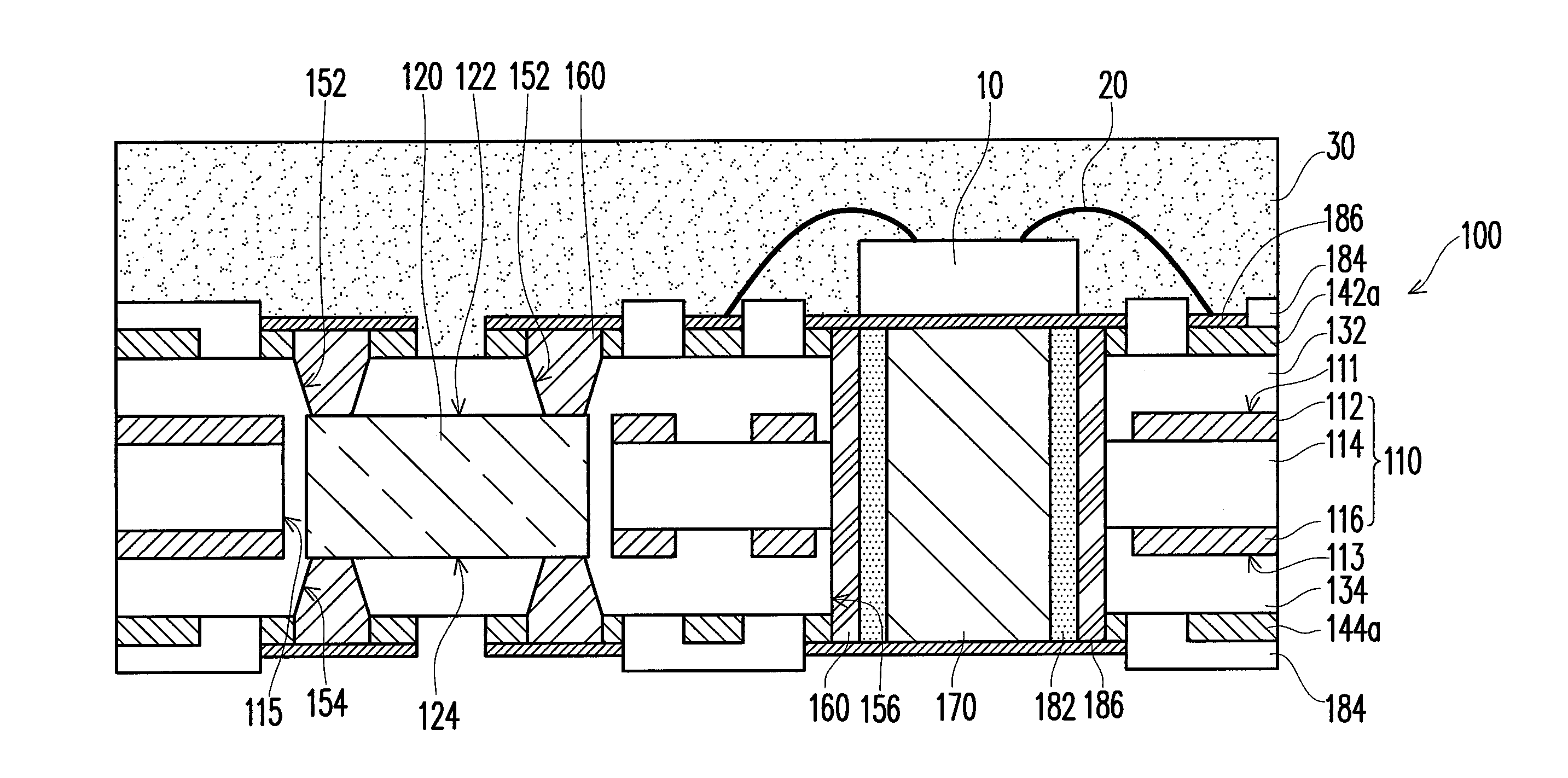
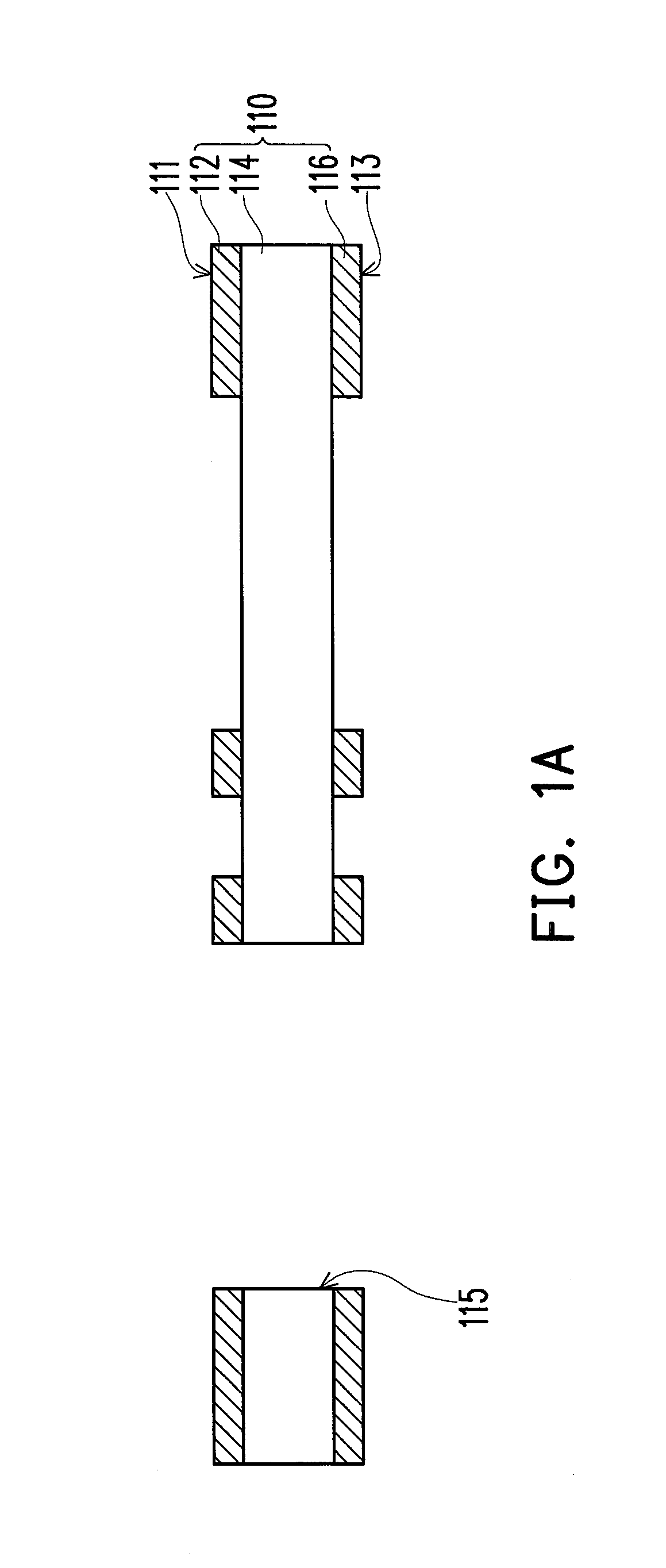
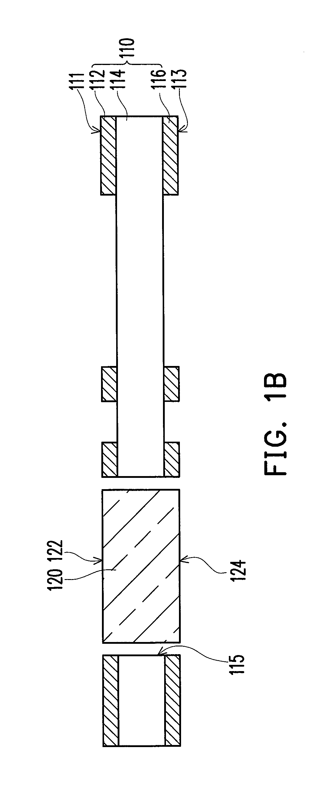
[0024]FIG. 1A to FIG. 1G are schematic cross-sectional views illustrating a manufacturing method of a package carrier according to an embodiment of the invention. As shown in FIG. 1A, in the manufacturing method of the package carrier according to the present embodiment, a substrate 110 is provided. The substrate 110 has an upper surface 111, a lower surface 113 opposite to the upper surface 111, and an opening 115 communicating the upper surface 111 and the lower surface 113. According to the present embodiment, the substrate 110 is composed of a first copper foil layer 112, a core dielectric layer 114, and a second copper foil layer 116, for instance, and the core dielectric layer 114 is disposed between the first copper foil layer 112 and the second copper foil layer 116. That is, the substrate 110 described in the present embodiment is a double-sided board. Certainly, in other embodiments, the substrate 110 may be a multi-layer board or a glass fiber (FR4) substrate. The type of...
PUM
 Abstract
Description
Claims
Application Information