Trenched semiconductor structure

a semiconductor structure and trenching technology, applied in the direction of semiconductor devices, basic electric elements, electrical appliances, etc., can solve the problems of low reverse breakdown voltage and high reverse leakage current of conventional semiconductor structures, and achieve the effect of increasing reverse breakdown voltage and reducing reverse leakage curren

Active Publication Date: 2013-10-17
TAIWAN SEMICONDUCTOR COMPANY LIMITED
View PDF3 Cites 13 Cited by
  • Summary
  • Abstract
  • Description
  • Claims
  • Application Information

AI Technical Summary

Benefits of technology

[0025]Accordingly, it is a main object of the present invention to provide a trenched semiconductor structure with active region trenches and a termination region trench formed in the epitaxial layer thereof. A depth of the termination region trench is greater than that of the active region trenches and close to a depth of the depletion region under reverse breakdown so as to achieve the effects of reducing reverse leakage current and increasing reverse breakdown voltage.

Problems solved by technology

In view of prior art, there exists a problem of high reverse leakage current and low reverse breakdown voltage of the conventional semiconductor structures because the ability to withstand the reverse breakdown voltage of the semiconductor structure would be reduced by the large reverse leakage current under high reverse bias voltage resulted from the implantation of P-type ions in the termination region.

Method used


Image

  • Trenched semiconductor structure
  • Trenched semiconductor structure
  • Trenched semiconductor structure

Examples


Embodiment Construction

[0032]There are various embodiments of the composite regeneration membrane in accordance with the present invention, which are not repeated hereby. The preferred embodiment is mentioned in the following paragraph as an example. It should be understood by those skilled in the art that the preferred embodiments disclosed in the following paragraph are merely an example instead of restricting the scope of the invention itself.

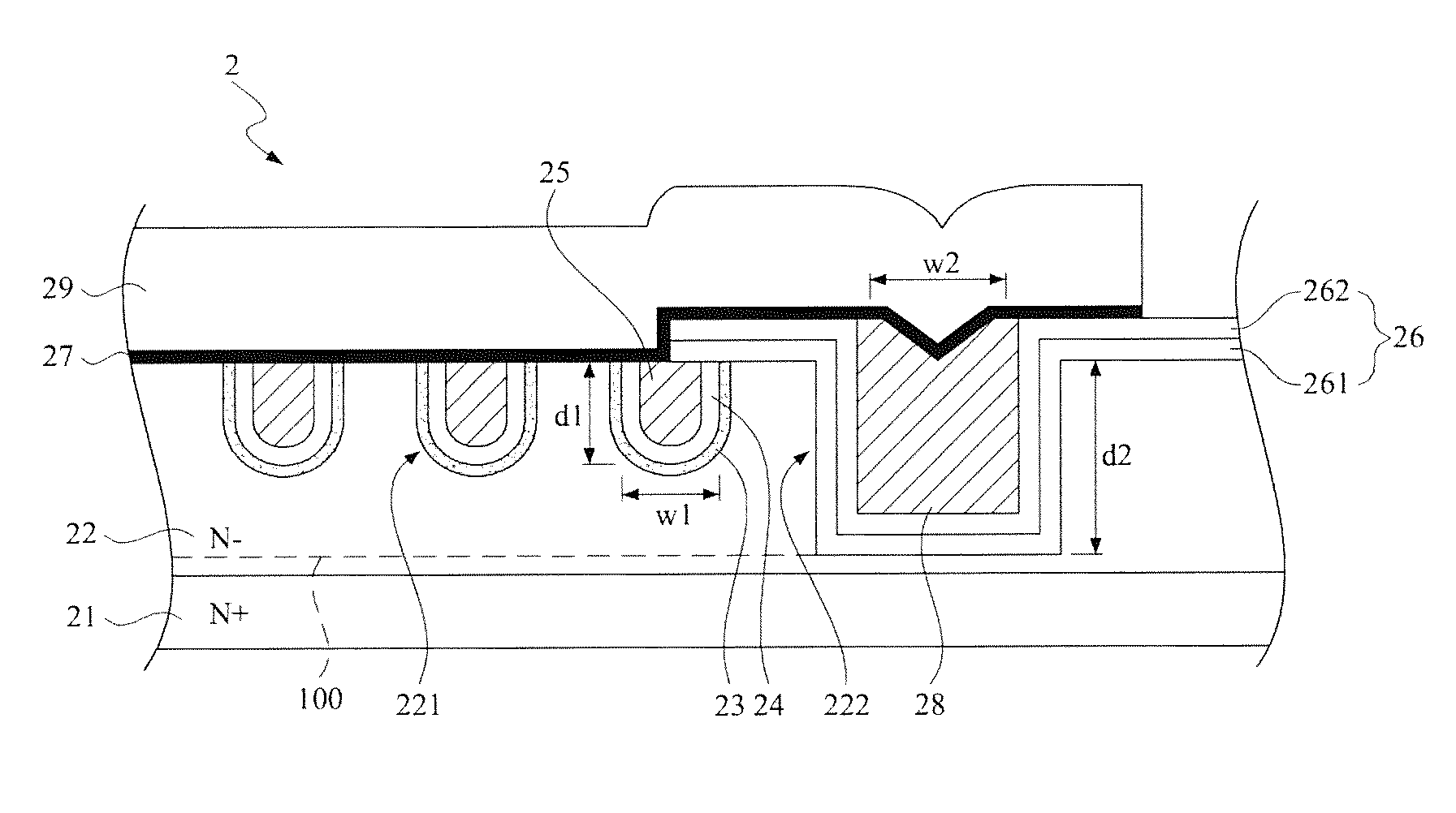
[0033]Referring to FIG. 3, which shows a cross section view of a semiconductor structure in accordance with a preferred embodiment of the present invention. As shown, the semiconductor structure 2 comprises a semiconductor substrate 21, an epitaxial layer 22, a plurality of ion implantation layers 23, an active region dielectric layer 24, a first polysilicon layer 25, a termination region dielectric layer 26, a schottky barrier layer 27, a second polysilicon layer 28, and a metal electrode layer 29.

[0034]The semiconductor substrate 21 is doped with impurities of a...


PUM


Abstract

A trenched semiconductor structure comprises a semiconductor substrate, an epitaxial layer, an ion implantation layer, a termination region dielectric layer, an active region dielectric layer, and a first polysilicon layer. The epitaxial layer doped with impurities of a first conductive type is formed on the semiconductor substrate. A plurality of active region trenches and a termination region trench are formed in the epitaxial layer. The ion implantation layer is formed in the active region trenches by doping impurities of a second conductive type. The termination region dielectric layer covers the termination region trench. The active region dielectric layer covers the ion implantation region. The first polysilicon layer covers the active region dielectric layer and fills the active region trenches. The depth of the termination region trench is greater than that of the active region trenches and close to that of the depletion region under reverse breakdown.

Description

FIELD OF THE INVENTION[0001]The present invention relates to a trenched semiconductor structure, and more particularly to a trenched structure with an epitaxial layer including an active region trenched and a termination region trench with a depth greater than the depth of the active region trenched and close to the depth of depletion region under reverse breakdown.BACKGROUND OF THE INVENTION[0002]Schottky diode is an important power device featuring a metal-semiconductor junction to create a schottky barrier for the purpose of rectification for a long time. With the characteristics of high switching speed and rectification, the schottky diode has been widely applied to high speed switching power devices, digital computers, and output regulators.[0003]However, the schottky diodes fabricated by using semiconductor structures in present has the disadvantages of low reverse breakdown voltage and large reverse leakage current. In addition, the reverse current increases with increasing t...

Claims


Application Information

Patent Timeline
Patent Type & Authority Applications(United States)
IPC IPC(8): H01L29/872
CPCH01L29/872H01L21/26586H01L29/0619H01L29/0661H01L29/407H01L29/47H01L29/8725
Inventor HUANG, CHAO-HSINCHUANG, CHIH-CHIANG
Owner TAIWAN SEMICONDUCTOR COMPANY LIMITED
Why Eureka
Try Eureka