Nitride semiconductor device

a nitride semiconductor and gate insulating film technology, applied in the direction of semiconductor devices, basic electric elements, electrical appliances, etc., can solve the problems of deterioration of character, loss of intrinsic advantages of nitride semiconductors, and difficulty in protecting gate insulating films, etc., to achieve the effect of improving reliability

Active Publication Date: 2013-11-07
FUJI ELECTRIC CO LTD +1
View PDF1 Cites 38 Cited by
  • Summary
  • Abstract
  • Description
  • Claims
  • Application Information

AI Technical Summary

Benefits of technology

[0034]The effect is achieved that there can be provided a nitride semiconductor device that preve

Problems solved by technology

Moreover, even if the gate insulating film 1022 is not broken, if a large voltage is continually applied to the drain electrode 1026 over a long period of time, there are cases in which there arises the problem of reliability such that a high electrical field is applied to the gate insulating film 1022 over a long period of time, and the characteristic thereof deteriorates over time.
However, when the concentration of the 2DEG is lowered, the conduction resistance of the 2DEG layer 1018 portion becomes large, and therefore, the on resistance of the element on the whole rises, and there is the drawback that the intrinsic advantages of a nitride semiconductor are lost.
However, it has become clear that, with this means, in a case in which the electron concentration of the 2DEG is greater than or equal to 3×1012 cm−2, it is difficult to protect the gate insulating film 1022.
However, it is

Method used


Image

  • Nitride semiconductor device
  • Nitride semiconductor device
  • Nitride semiconductor device

Examples


first embodiment

[0058]A nitride semiconductor device of the present embodiment is described in detail hereinafter with reference to the drawings. Note that the present embodiment is an example of the semiconductor device of the present invention, and the present invention is not limited by the present embodiment.

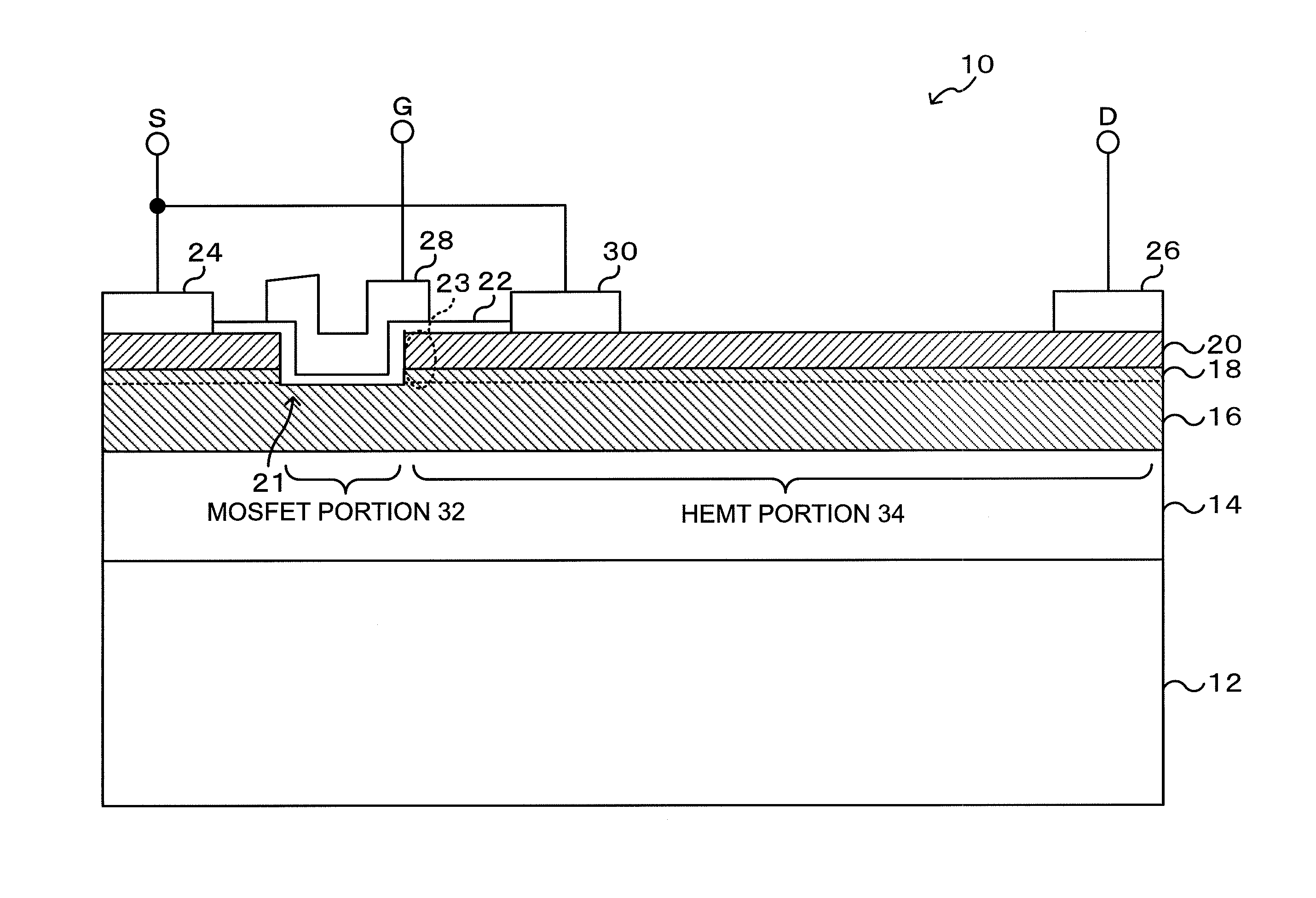
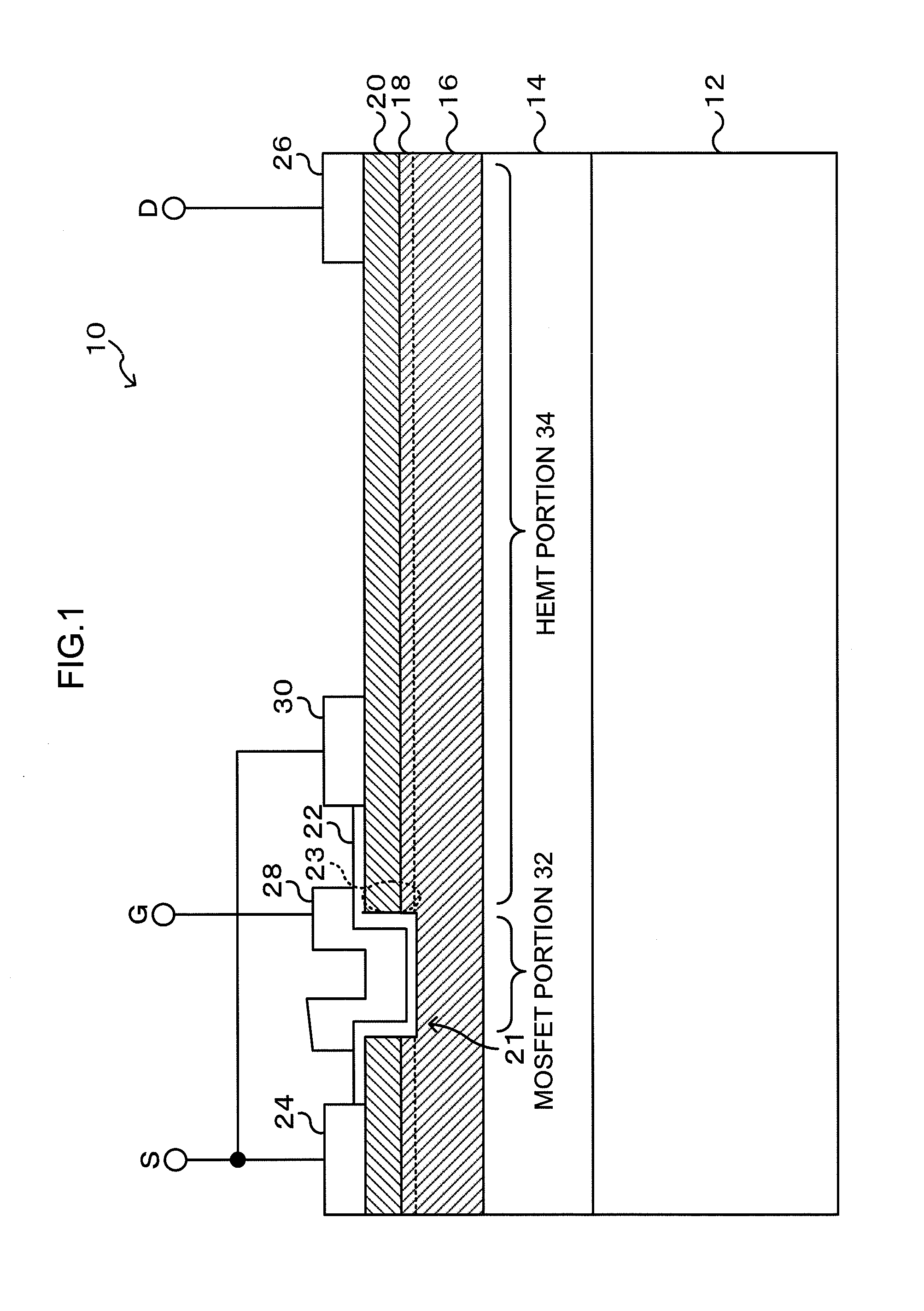
[0059]A cross-sectional view showing an example of the schematic structure of a nitride semiconductor element, that is the nitride semiconductor device of the present embodiment, is shown in FIG. 1.

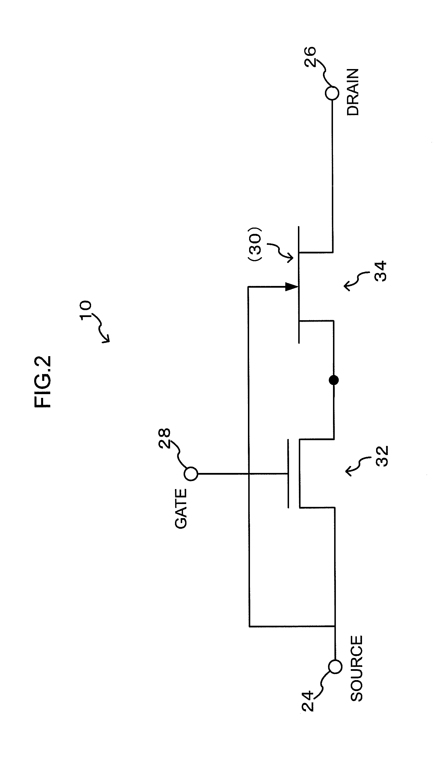
[0060]A nitride semiconductor element 10 of the present embodiment is structured to have a substrate 12, a buffer layer 14, a GaN layer 16, an AlGaN layer 20, a gate insulating film 22, a source electrode 24, a gate electrode 28, a drain electrode 26, the gate electrode 28, and an SBD (Schottky Barrier Diode) metal electrode 30. Further, when viewed as equivalent circuits, the nitride semiconductor element 10 of the present embodiment is structured from a MOSFET portion 32 and an HEMT (High Elect...

second embodiment

[0096]A nitride semiconductor element of a second embodiment has a structure and operation that are substantially similar to those of the nitride semiconductor element 10 of the first embodiment. Therefore, the same portions are denoted by the same reference numerals and detailed description thereof is omitted, and only the portions that differ are described in detail.

[0097]A cross-sectional view, that shows an example of the schematic structure of a nitride semiconductor element that is a nitride semiconductor device of the present embodiment, is shown in FIG. 7. In a nitride semiconductor element 50 of the present embodiment, a recess portion 51 is formed so as to not reach the GaN layer 16, i.e., such that the portion beneath the MOSFET portion 32 is the AlGaN layer 20. Structuring the nitride semiconductor element in this way is preferable in cases in which the threshold value of the MOSFET portion 32 may be made to be low to a certain extent. Note that, in the present embodimen...

third embodiment

[0100]A nitride semiconductor element of a third embodiment has a structure and operation that are substantially similar to those of the nitride semiconductor element 10 of the first embodiment and the nitride semiconductor element 50 of the second embodiment. Therefore, the same portions are denoted by the same reference numerals and detailed description thereof is omitted, and only the portions that differ are described in detail.

[0101]A cross-sectional view, that shows an example of the schematic structure of a nitride semiconductor element that is a nitride semiconductor device of the present embodiment, is shown in FIG. 8. In the nitride semiconductor element 10 of the first embodiment, the SBD metal electrode 30 is provided as an electrode that is Schottky-joined to the AlGaN layer 20. However, in a nitride semiconductor element 60 of the present embodiment, instead of this, a p-AlGaN layer 64 (semiconductor layer) that is pn-joined to the AlGaN layer 20, and an electrode that...


PUM


Abstract

The present invention prevents breakage of a gate insulating film of a MOS device and provides a nitride semiconductor device having improved reliability. An SBD metal electrode provided between a drain electrode and a gate electrode is configured to form a Schottky junction with an AlGaN layer. Further, the SBD metal electrode and a source electrode are connected and electrically short-circuited. Consequently, when an off signal is inputted to the gate electrode, a MOSFET part is turned off and the drain-side voltage of the MOSFET part becomes close to the drain electrode voltage. When the drain electrode voltage increases, the SBD metal electrode voltage becomes lower than the drain-side voltage of the MOSFET part, thus the drain side of the MOSFET part and the drain electrode are electrically disconnected by the SBD metal electrode.

Description

TECHNICAL FIELD[0001]The present invention relates to a normally-off nitride semiconductor device having a MOS structure.BACKGROUND ART[0002]Conventionally, a gallium nitride (GaN) compound semiconductor device (hereinafter called a GaN semiconductor element) is used as a semiconductor material in semiconductor elements for high-frequency devices. In a GaN semiconductor element, a buffer layer formed by using, for example, a Metal-Organic Chemical Vapor Deposition (MOCVD) method, and an electron traveling layer that is doped with impurities, are provided on the surface of a substrate. Recently, because it has been recognized that GaN semiconductor elements can be applied as well to semiconductor devices for power (power devices) in addition to high-frequency applications, studies are being carried out on GaN semiconductor elements that handle high withstand voltages and large currents.[0003]A gallium nitride semiconductor element having a MOS structure is disclosed in Patent Documen...

Claims


Application Information

Patent Timeline
IPC IPC(8): H01L29/778H01L29/20
CPCH01L29/778H01L29/2003H01L29/402H01L29/407H01L29/42316H01L29/42376H01L29/66462H01L29/7787
Inventor UENO, KATSUNORIKAYA, SHUSUKE
Owner FUJI ELECTRIC CO LTD
Why Eureka
Try Eureka