Semiconductor device

a semiconductor device and memory technology, applied in the direction of memory address/allocation/relocation, instruments, climate sustainability, etc., can solve the problems of extremely lowering the performance of the cache memory, and reducing the reliability of the semiconductor device. , the effect of lowering the reliability of the semiconductor devi

Inactive Publication Date: 2013-11-07
SEMICON ENERGY LAB CO LTD
View PDF6 Cites 16 Cited by
  • Summary
  • Abstract
  • Description
  • Claims
  • Application Information

AI Technical Summary

Benefits of technology

[0037]According to one embodiment of the present invention, the frequency of access to a cache memory is monitored, and supplying the power supply voltage to a CPU is stopped in the case where the frequency of access is uniform. Alternatively, in the case where the frequency of access is not uniform, the stop of supplying the power supply voltage is performed on memories with a time interval; eventually, the supply of the power ...

Problems solved by technology

However, the content of data stored in a cache memory is lost at the same time as the stop of power supply.
Without consideration of timing, power gating is performed, for example, in a state where access to the cache memory is frequently performed, which causes an extremely lowering of performance of the cache memory.
According to Patent Document 1, by utilizing a transition period du...

Method used


Image

  • Semiconductor device
  • Semiconductor device
  • Semiconductor device

Examples


embodiment 1

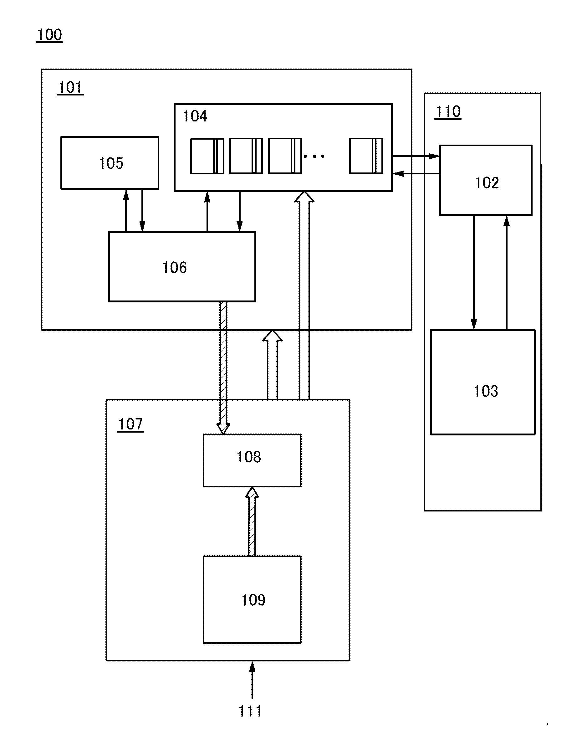
[0053]In this embodiment, a structure of a semiconductor device in which an n-way set associative cache memory is used will be described as an example with reference to FIG. 1. In the semiconductor device, the frequency of access to the cache memory is monitored, and with consideration of conditions of the cache memory in accordance with monitoring results, supply of the power supply voltage to the CPU can be stopped by a power supply control circuit. Further, by utilizing determination of a dirty bit in the cache memory, high-efficiency write back processing whose processing time is shortened can be performed.

[0054]A semiconductor device 100 includes a CPU 101, a memory device 110, and a power supply control circuit 107. In the CPU 101, a cache memory 104, a register 105, and an arithmetic circuit 106 are provided. In the memory device 110, a main memory device 102 and an auxiliary memory device 103 are provided. In the power supply control circuit 107, a setup register 108 and a c...

embodiment 2

[0162]As described in Embodiment 1, in the semiconductor device according to one embodiment of the present invention, data of all the valid bits is set to Data A when supply of the power supply voltage to the CPU is resumed. Immediately after the supply of the power supply voltage to the CPU is resumed by the setting of the valid bits, cache miss frequently occurs. However, while instructions and data necessary for arithmetic processing executed immediately after resuming the supply of the power supply voltage to the CPU are gradually stored in the cache memory, the arithmetic processing can restart. Thus, the arithmetic processing of the CPU can be restarted at high speed as compared with the case where arithmetic processing is not restarted until all data in the cache memory is restored. By shortening the processing time necessary for the CPU to restart the arithmetic processing, a period during which the supply of the power supply voltage is stopped is made longer, and power cons...

embodiment 3

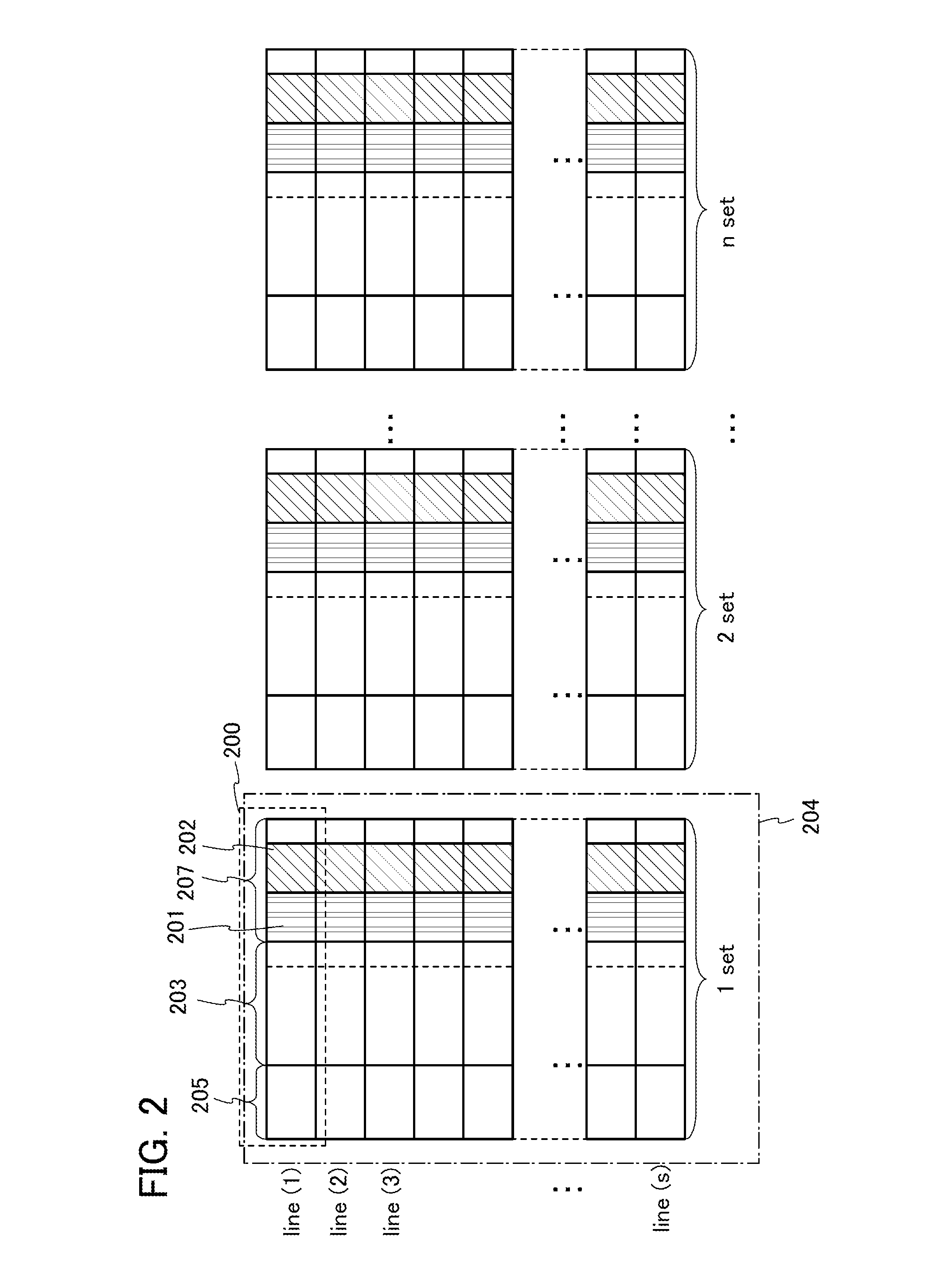
[0173]In this embodiment, an example of a structure of the cache memory described in Embodiment 1 will be described with reference to FIG. 12A. Specifically, an example in which a cache memory is formed with an SRAM in which a flip-flop circuit is used in a memory portion is described. In addition, an example of a structure of the memory device (e.g., the main memory) outside the CPU described in Embodiment 1 is described with reference to FIG. 12B. Specifically, an example in which a memory device outside the CPU is formed with a DRAM is described.

[0174]In a portable information terminal such as a mobile phone, a smartphone, or an electronic book, an SRAM or a DRAM is frequently used so as to store image data or the like temporarily. In a semiconductor device according to one embodiment of the present invention, an SRAM whose access rate is high is preferably used for the cache memory. Further, a DRAM with higher capacitance is preferably used for the main memory device.

[0175]FIG. ...


PUM


Abstract

To provide a semiconductor device with less power consumption. In a semiconductor device including a CPU, the frequency of access to a cache memory is monitored. In the case where the access frequency is uniform, supply of a power supply voltage to the CPU is stopped. In the case where the access frequency is not uniform, stop of supplying the power supply voltage is performed on memories with a time interval, and eventually, supply of the power supply voltage to the CPU is stopped. Further, write back processing is efficiently performed in accordance with determination of a dirty bit, so that power consumption of the semiconductor device can be further achieved.

Description

BACKGROUND OF THE INVENTION[0001]1. Field of the Invention[0002]The present invention relates to a semiconductor device. In particular, the present invention relates to a semiconductor device whose power consumption is reduced by stopping supply of the power supply voltage to a CPU.[0003]In this specification, a semiconductor device generally means a device which can function by utilizing semiconductor characteristics, and an electrooptic device, a semiconductor circuit, and electronic equipment are all semiconductor devices.[0004]2. Description of the Related Art[0005]Most computers currently used are von Neumann computers employing a stored-program system. The stored-program system is such a system that data necessary for arithmetic processing is stored in a memory device outside a CPU and the data is sequentially read out. To improve performance of arithmetic processing, as well as an increase in an operation speed of the CPU, an increase in speed of loading and storing the data ...

Claims


Application Information

Patent Timeline
IPC IPC(8): G06F12/08
CPCG06F12/0802G06F1/3225G06F1/3287Y02D10/00
Inventor KUROKAWA, YOSHIYUKI
Owner SEMICON ENERGY LAB CO LTD
Why Eureka
Try Eureka