Liquid crystal device and electronic apparatus

a technology of electronic equipment and liquid crystal, which is applied in the direction of instruments, non-linear optics, optics, etc., can solve the problems of deterioration of display characteristics, increase in production costs, and productivity decline, and achieve high display quality and reliability

Inactive Publication Date: 2013-11-14
SEIKO EPSON CORP
View PDF3 Cites 4 Cited by
  • Summary
  • Abstract
  • Description
  • Claims
  • Application Information

AI Technical Summary

Benefits of technology

[0031]According to this configuration, the electronic apparatus can be provided that has a high display quality and reliability.

Problems solved by technology

It is known that in this process of manufacturing the liquid crystal device, when ionic impurities, for example, are mixed in at the time of liquid crystal injection, or flows out of a sealant surrounding a liquid crystal layer, the ionic impurities are diffused into and coagulated (unevenly-distributed) into a display region, thereby causing deterioration in display characteristics.
Furthermore, adjustment of a drive voltage (a drive waveform) is necessary, and there is a problem, such as a concern that this invites an increase in production cost and a decrease in the productivity.
According to this configuration, even though the decrease in the display quality resulting from the orientation disorder of the liquid crystal molecule in the vicinity of the protrusion portion occurs, it is possible to make it difficult for this to be noticeable.

Method used


Image

  • Liquid crystal device and electronic apparatus
  • Liquid crystal device and electronic apparatus
  • Liquid crystal device and electronic apparatus

Examples


first embodiment

[0048]According to a first embodiment, an active matrix type liquid crystal device, equipped with a thin film transistor (TFT) as a switching element of a pixel, is described as an example. The liquid crystal device also can be suitably used, for example, as a light modulation element (a liquid crystal light valve) of a projection type display apparatus (a liquid crystal projector) described below.

Liquid Crystal Device

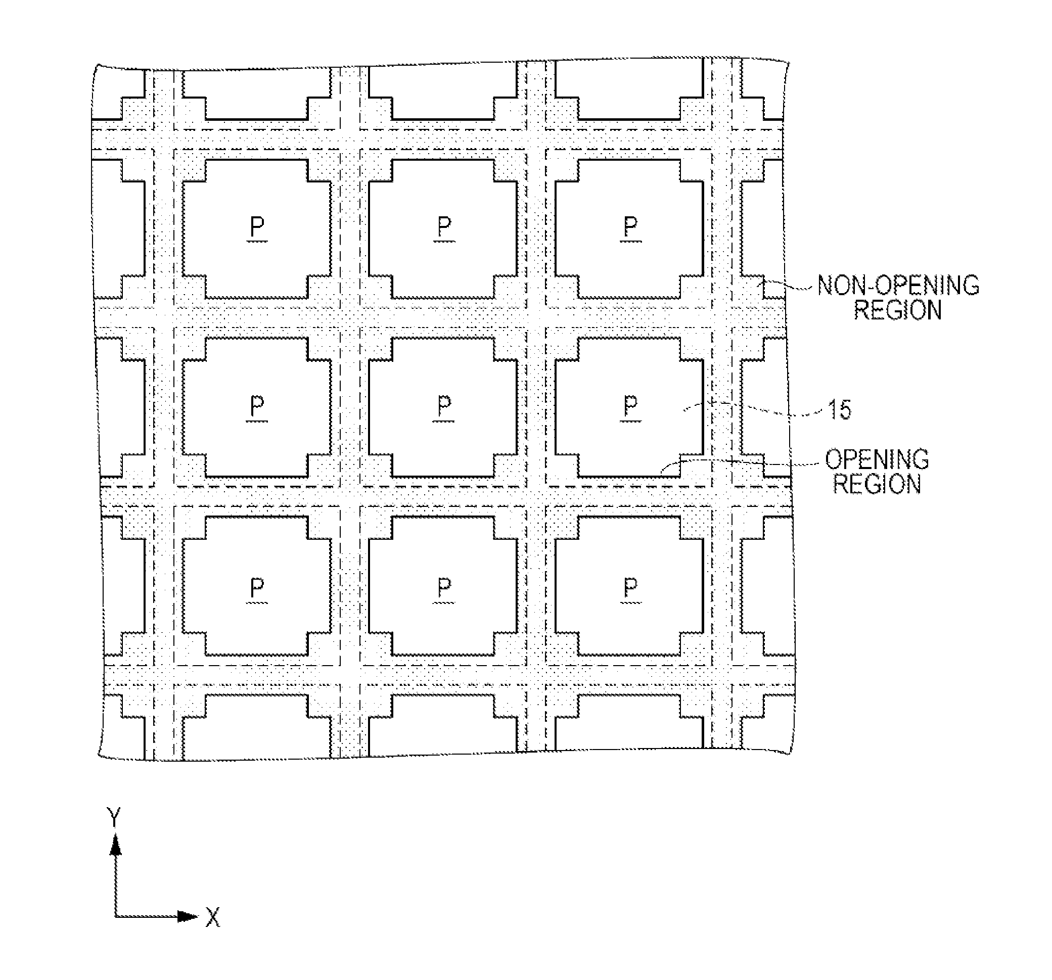
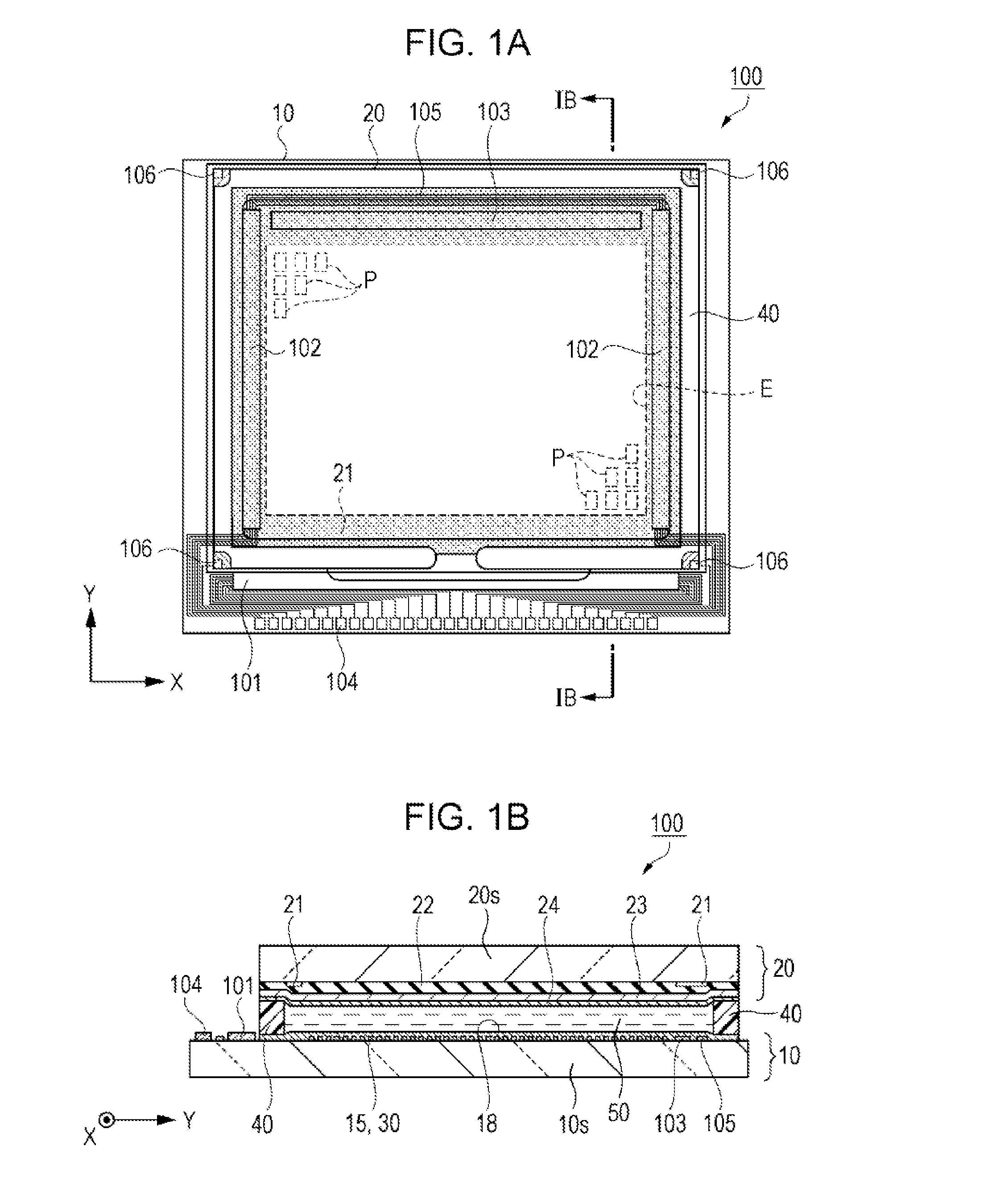
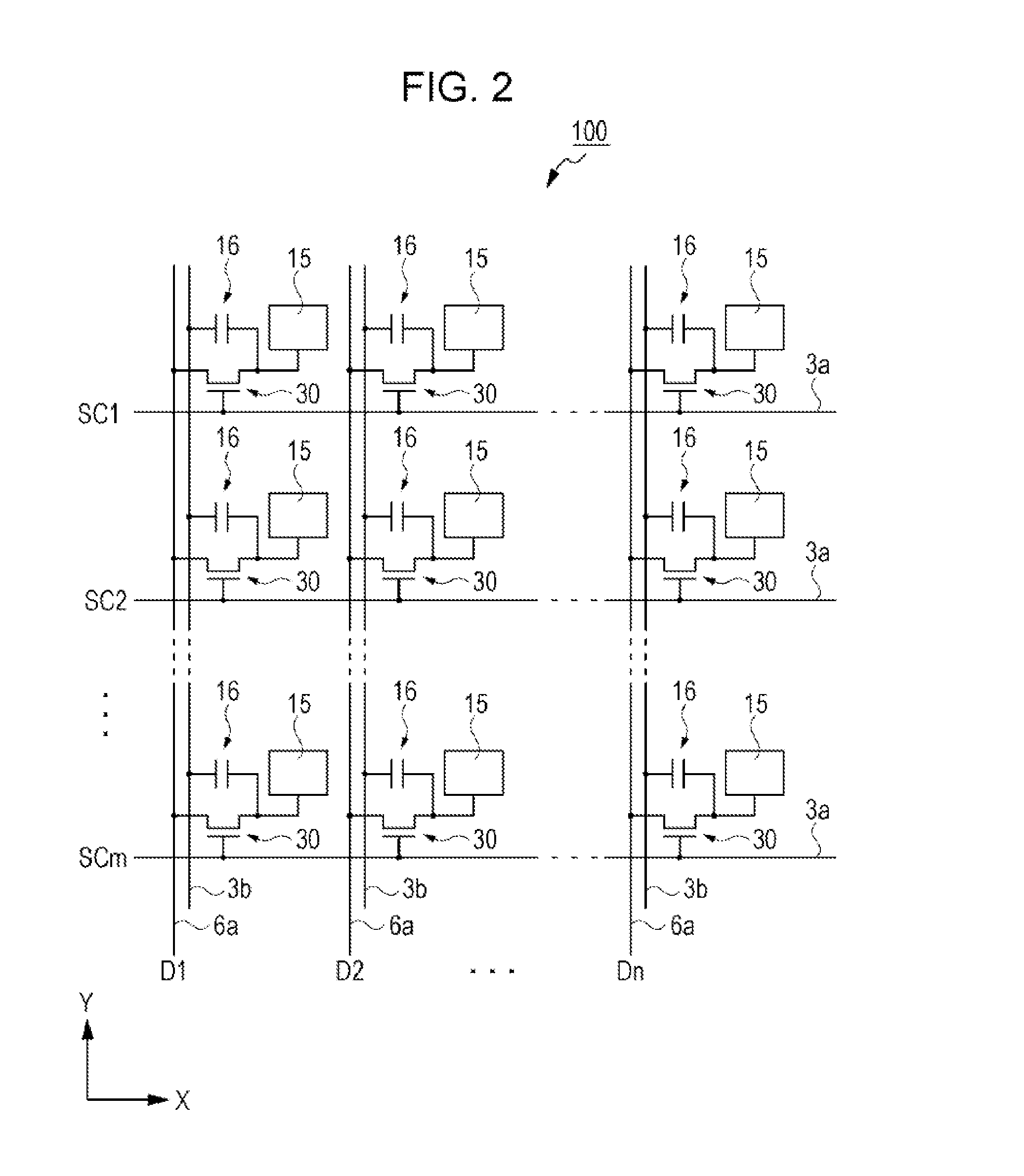
[0049]First, the liquid crystal device according to the first embodiment is described referring to FIGS. 1A and 1B and 2. FIG. 1A is a schematic plan view illustrating a configuration of the liquid crystal device, and FIG. 1B is a schematic cross-sectional view that is taken along a line IB-IB across the liquid crystal device in FIG. 1A. FIG. 2 is a diagram of an equivalent circuit illustrating an electrical configuration of the liquid crystal device.

[0050]A liquid crystal device 100 according to the first embodiment, as illustrated in FIGS. 1A and 1B, has an element s...

second embodiment

[0119]Next, a liquid crystal device according to a second embodiment is described referring to FIGS. 11A and 11B. FIG. 11A is a schematic plan view illustrating a configuration of a protrusion portion in the liquid crystal device according to the second embodiment, and FIG. 11B is a schematic cross-sectional view that is taken along a line XIB-XIB passing through the protrusion portion at an inclination angle of 45 from lower left to upper right in FIG. 11A. That is, the line XIB-XIB is along a deposition direction (an inclination direction (a flow direction) of the liquid crystal molecule LC)) in an oblique deposition of an orientation film 18 in an element substrate 10.

[0120]The liquid crystal device according to the second embodiment is a liquid crystal device that results from providing the protrusion portion on the side of the opposite substrate 20 in the liquid crystal device 100 according to the first embodiment. Therefore, the same configurations as that according to the fir...

third embodiment

Electronic Apparatus

[0129]Next, an electronic apparatus according to a third embodiment is described referring to FIG. 12. FIG. 12 is a schematic diagram illustrating a configuration of a projection type display apparatus as an electronic apparatus.

[0130]As illustrated in FIG. 12, a projection type display apparatus 1000 as the electronic apparatus according to the third embodiment includes a polarized-light emission device 1100 that is arranged along a system optical axis L, two dichroic mirrors 1104 and 1105, as light separation elements, three reflection mirrors 1106, 1107, and 1108, five relay lenses 1201, 1202, 1203, 1204, and 1205, transmission type liquid crystal light valves 1210, 1220, and 1230, as three light modulation units, cross dichroic prism 1206, as a photosynthesis element, and a projection lens 1207.

[0131]The polarized-light emission device 1100 is mainly configured from a lamp unit 1101, as a light source that is made from a white light source, such as an ultrahi...


PUM

PropertyMeasurementUnit
heightaaaaaaaaaa
voltageaaaaaaaaaa
pre-tilt angle θpaaaaaaaaaa

Abstract

There is provided a liquid crystal device including a first substrate, a second substrate, a liquid crystal layer that is interposed between and supported by the first substrate and the second substrate, a protrusion portion that is provided on the first substrate and protrudes toward the liquid crystal layer, and a plurality of pixel electrodes that are arranged in the vicinity of the protrusion portion. In the liquid crystal device, a spacing between ends of the plurality of pixel electrodes and an end of the protrusion portion is greater than a height of the protrusion portion.

Description

BACKGROUND[0001]1. Technical Field[0002]The present invention relates to a liquid crystal device and an electronic apparatus.[0003]2. Related Art[0004]Generally, a liquid crystal device has a construction in which liquid crystal is injected and enclosed between a pair of substrates on which orientation processing is performed. It is known that in this process of manufacturing the liquid crystal device, when ionic impurities, for example, are mixed in at the time of liquid crystal injection, or flows out of a sealant surrounding a liquid crystal layer, the ionic impurities are diffused into and coagulated (unevenly-distributed) into a display region, thereby causing deterioration in display characteristics.[0005]For example, JP-A-2008-58497 discloses the liquid crystal display device in which in order to suppress the deterioration in display characteristics resulting from the ionic impurities, in the pair of substrates, one substrate includes a pixel electrode formed in a pixel regio...

Claims


Application Information

Patent Timeline
Patent Type & Authority Applications(United States)
IPC IPC(8): G02F1/1343G02F1/1337G02F1/1333
CPCG02F1/134336G02F1/133345G02F1/1337G02F1/133707G02F2201/40
Inventor EGAMI, TAKAFUMI
Owner SEIKO EPSON CORP
Why Eureka
Try Eureka