Lasers with beam-shape modification

a technology of beam shape and laser, which is applied in the field of photonic devices, can solve the problems of laser characteristics degradation, process complexity and degradation of laser characteristics, and the inability of conventional lithographic techniques to be used to further process lasers

Active Publication Date: 2013-11-14
MACOM TECH SOLUTIONS HLDG INC
View PDF18 Cites 13 Cited by
  • Summary
  • Abstract
  • Description
  • Claims
  • Application Information

AI Technical Summary

Problems solved by technology

Since the semiconductor material is cleaved to form the laser facets, the locations and orientations of the facets are limited; furthermore, once the wafer has been cleaved, typically it is in small pieces so that conventional lithographical techniques cannot readily be used to further process the lasers.
One of the major challenges in the use of semiconductor lasers is the mismatch between the output beam from the laser and the medium to which the beam is directed or coupled.
For example, forming a semiconductor laser with spot size converters (SSC) can allow more efficient coupling of the laser light to an optical fiber or expand the tolerance for optical alignment, however, in general there are certain disadvantages that come along with forming SSC, such as process complexity and degradation in laser characteristics.

Method used


Image

  • Lasers with beam-shape modification
  • Lasers with beam-shape modification
  • Lasers with beam-shape modification

Examples


Embodiment Construction

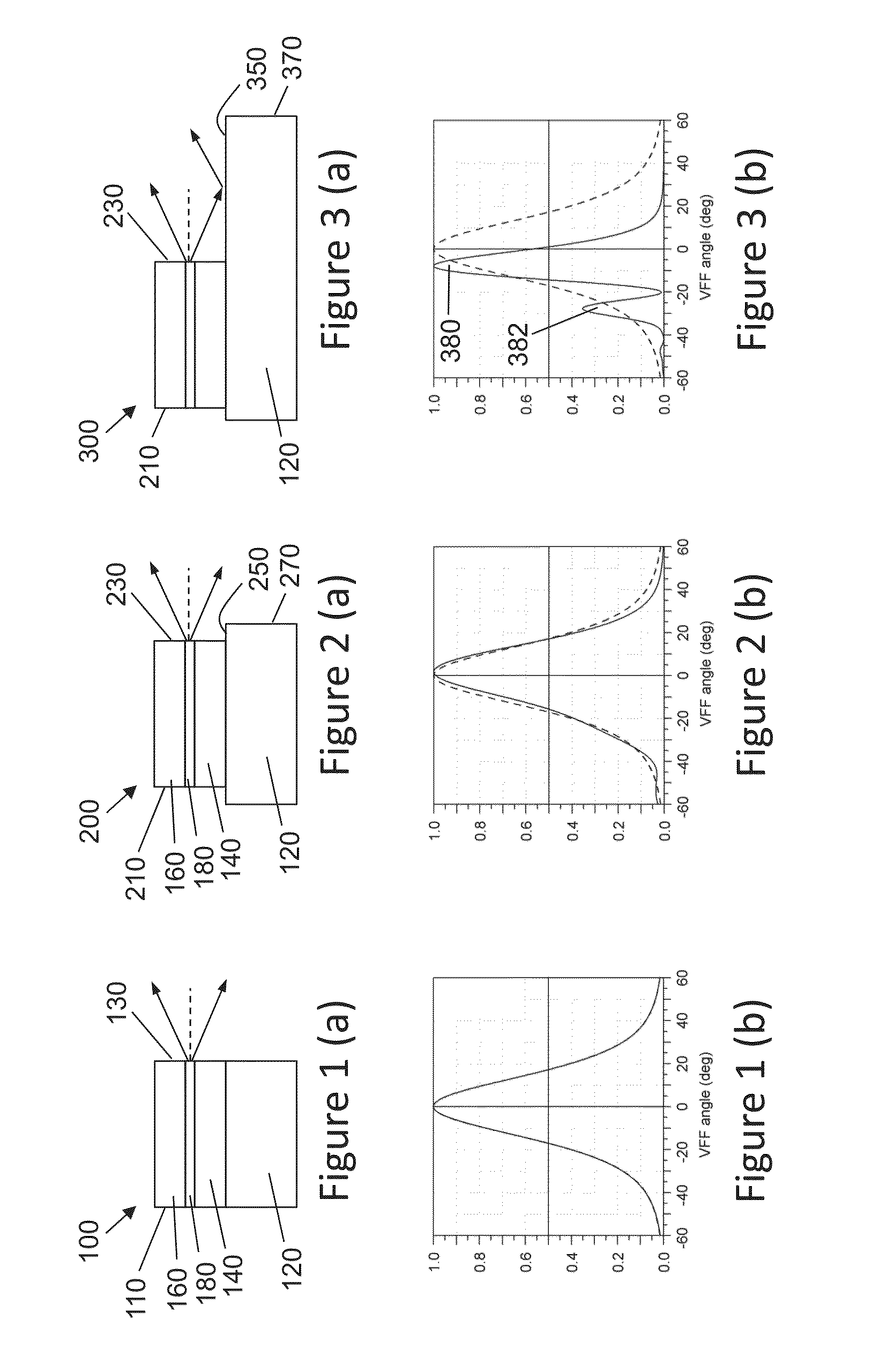
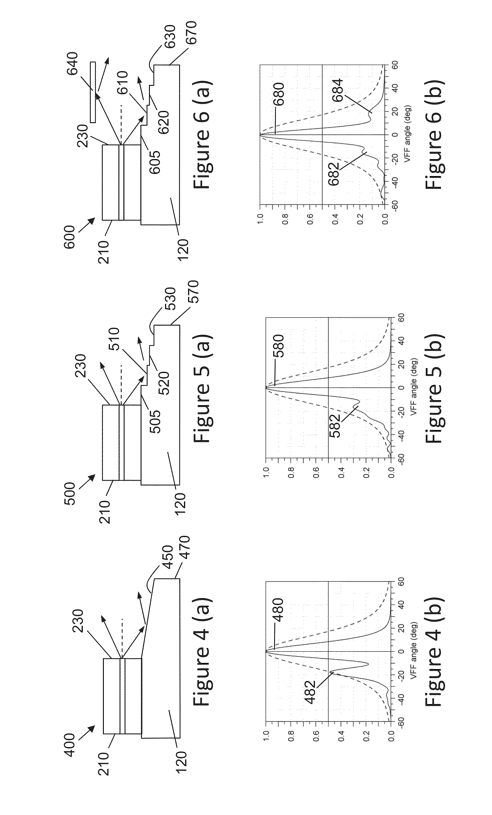
[0031]FIG. 1 (a) shows a semiconductor laser 100 formed through cleaving of the front 130 and back 110 facets. The laser structure comprises a substrate 120 with epitaxially deposited layers that allow the formation of a lower cladding layer 140, which may extend into the substrate or be completely epitaxially deposited as shown in FIG. 1 (a) and of thickness 1.83 μm, an active region 180 of 0.34 μm thickness, and an upper cladding layer 160 of 1.83 μm. The laser emits laser light at around 1310 nm. FIG. 1 (b) shows the vertical far-field (VFF) obtained through RSoft Finite-Difference Time-Domain (FDTD) simulations from either the front or back facet of the structure in FIG. 1 (a).

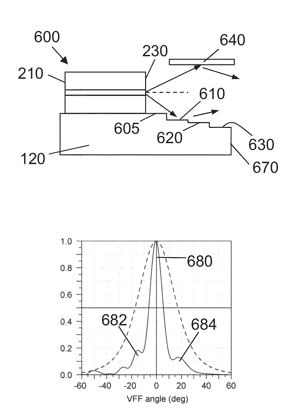
[0032]FIG. 2 (a) shows a cross-section of a semiconductor laser 200 formed through etching of the front 230 and back facets 210 at or close to perpendicular to the plane of the substrate 120, which is usually a deviation of the etched facet of up to 3° from the normal to the plane of the substrate. Example...


PUM


Abstract

A beam control structure for semiconductor lasers that allows modification of the shape of a beam allowing, for example, higher coupling into an optical fiber. The structure may comprise one or more of a tilted patio, a staircase, a reflective roof, and a reflective sidewall.

Description

CROSS-REFERENCE TO RELATED APPLICATIONS[0001]This patent application claims priority to U.S. Provisional Patent Application No. 61 / 644,270, filed May 8, 2012, which is hereby incorporated by reference herein in its entirety.BACKGROUND OF THE DISCLOSURE[0002]The present disclosure relates, in general, to photonic devices, and more particularly to improved photonic devices and methods for fabricating them.[0003]Semiconductor lasers typically are fabricated on a wafer by growing an appropriate layered semiconductor material on a substrate through Metalorganic Chemical Vapor Deposition (MOCVD) or Molecular Beam Epitaxy (MBE) to form an epitaxial structure having an active layer parallel to the substrate surface. The wafer is then processed with a variety of semiconductor processing tools to produce a laser optical cavity incorporating the active layer and incorporating metallic contacts attached to the semiconductor material. Laser facets are typically formed at the ends of the laser ca...

Claims


Application Information

Patent Timeline
Patent Type & Authority Applications(United States)
IPC IPC(8): H01S5/30H01S5/02315
CPCH01S5/3013H01S5/0217H01S5/02212H01S5/0267H01S5/22H01S5/34326H01S2301/18H01S5/1085B82Y20/00H01S5/0207H01S5/0235H01S5/02325H01S5/02251H01S5/02315H01S5/0233H01S5/0287
Inventor STAGARESCU, CRISTIANBEHFAR, ALEX A.KWONG, NORMAN SZE-KEUNG
Owner MACOM TECH SOLUTIONS HLDG INC
Why Eureka
Try Eureka