Eureka AIR delivers breakthrough ideas for toughest innovation challenges, trusted by R&D personnel around the world.

Method for forming patterns of dense conductor lines and their contact pads, and memory array having dense conductor lines and contact pads

Active Publication Date: 2013-11-21
NAN YA TECH
View PDF3 Cites 14 Cited by
  • Summary
  • Abstract
  • Description
  • Claims
  • Application Information

AI Technical Summary

Benefits of technology

The method described in this patent allows for the formation of dense conductor lines and their contact pads efficiently. By trimming and forming patterned lines, and then removing unnecessary parts, the method reduces the area required for reliable electrical contact and maximizes die-size efficiency. This is made possible by using derivative line patterns and chop patterns that allow for the simultaneous formation of multiple lines and pads. The method is effective in improving the die-space efficiency of the memory chip.

Problems solved by technology

However, the shark jaw layout takes much lateral area so that the integration degree of the devices is adversely affected.

Method used


Image

  • Method for forming patterns of dense conductor lines and their contact pads, and memory array having dense conductor lines and contact pads
  • Method for forming patterns of dense conductor lines and their contact pads, and memory array having dense conductor lines and contact pads
  • Method for forming patterns of dense conductor lines and their contact pads, and memory array having dense conductor lines and contact pads

Examples


Embodiment Construction

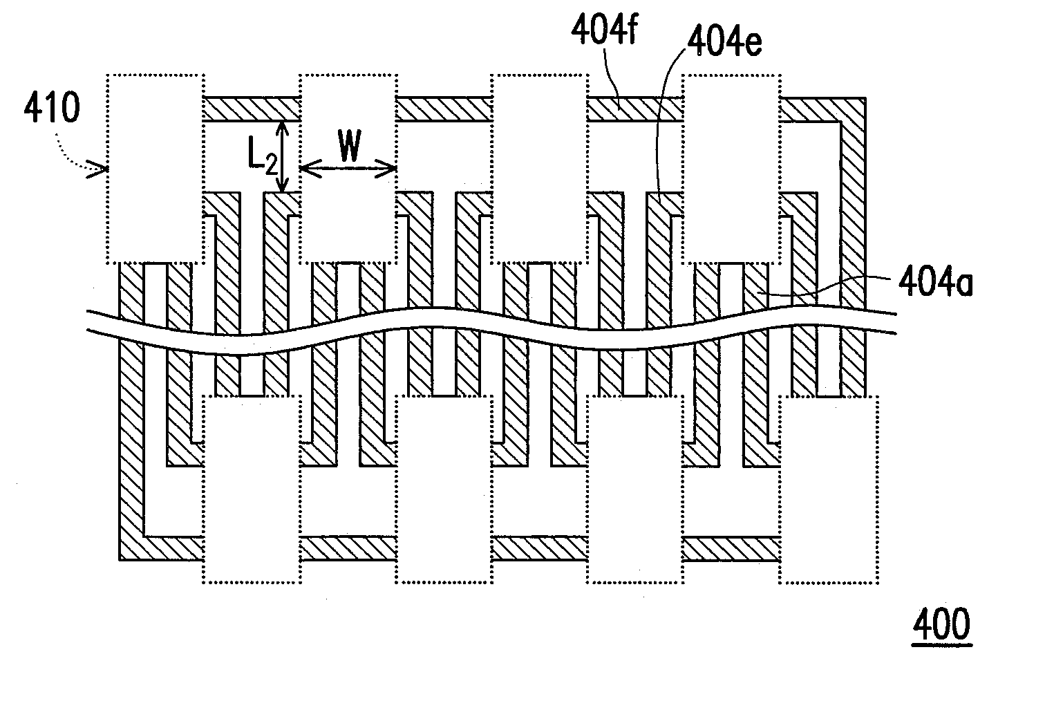
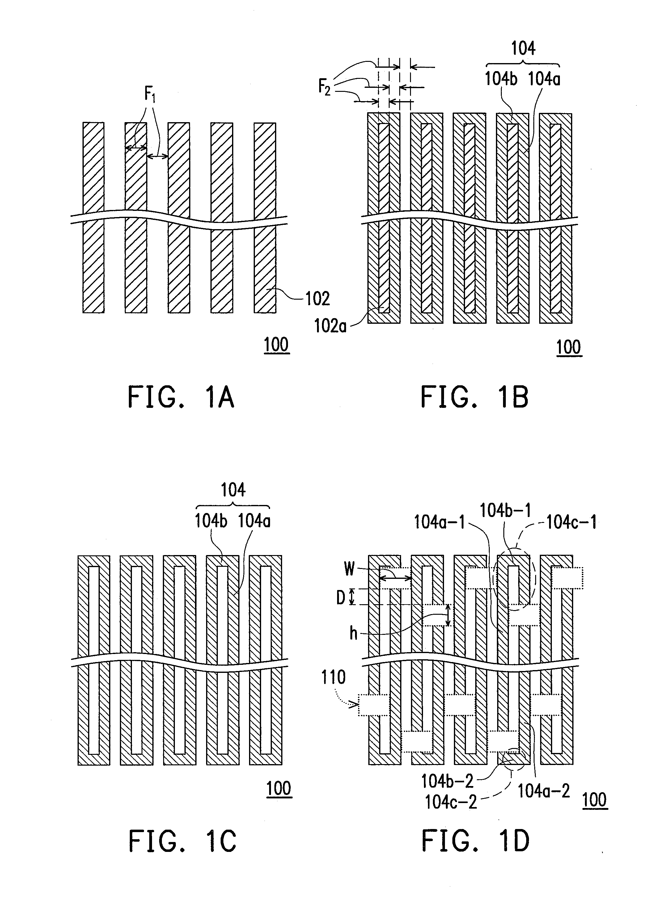
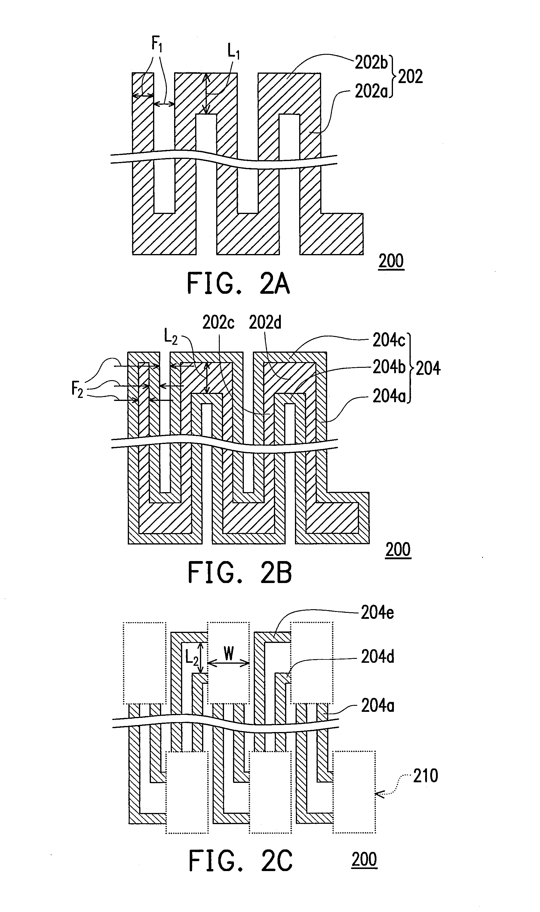
[0021]This invention is further explained with the following embodiments referring to the accompanying drawings, which are not intended to limit the scope of this invention.

[0022]FIGS. 1A-1D illustrate, in a top view, a method for forming patterns of dense conductor lines and their contact pads according to the first embodiment of this invention.

[0023]Referring to FIG. 1A, a plurality of parallel base line patterns 102 are defined lithographically over a substrate 100, possibly having a feature size of F1 and a pitch of 2F1. The substrate 100 may have thereon a conductive layer to be patterned into dense conductor lines and their contact pads, or may alternatively have thereon an underlying layer for the conductor lines and their contact pads that are formed later as portions of the derivative line patterns and derivative transverse patterns. The feature size F1 can be the lithography-limit feature size so that the derivative line patterns formed later can have a maximal density. Th...


PUM


Abstract

A method for forming patterns of dense conductor lines and their contact pads is described. Parallel base line patterns are formed over a substrate. Each of the base line patterns is trimmed. Derivative line patterns and derivative transverse patterns are formed as spaces on the sidewalls of the trimmed base line patterns, wherein the derivative transverse patterns are formed between the ends of the derivative line patterns and adjacent to the ends of the trimmed base line patterns. The trimmed base line patterns are removed. At least end portions of the derivative line patterns are removed, such that the derivative line patterns are separated from each other and all or portions of the derivative transverse patterns become patterns of contact pads each connected with a derivative line pattern.

Description

BACKGROUND OF THE INVENTION[0001]1. Field of Invention[0002]This invention relates to integrated circuit (IC) fabrication, and particularly to a method for forming patterns of dense conductor lines and their contact pads, and to a memory array having high density of conductor lines and contact pads.[0003]2. Description of Related Art[0004]The resolution in a photolithography process depends on the wavelength of the exposure light, the numerical aperture (NA) of the optical system and the design of the photomask, and has a limit of about ⅕ to ⅓ of the wavelength of the exposure light according to the exposure conditions. When the resolution required by an array of patterns exceeds the resolution of the lithographic system, for example, in a case of forming the gate line array of a high-density memory like a DRAM of next generation, a pitch reduction method is needed, mainly based on the spacer forming technique.[0005]For example, patterns of dense conductor lines beyond lithographic ...

Claims


Application Information

Patent Timeline
IPC IPC(8): H01L23/485H01L21/768
CPCH01L21/76892H01L2221/1068H10B12/30H10B12/485H01L2924/0002H01L21/76838H01L2924/00
Inventor DOEBLER, JONATHANSILLS, SCOTT
Owner NAN YA TECH
Why Eureka
Eureka Blog
Learn More